Timing generation circuit
A technology for generating circuits and circuits, applied to electrical components, drinking vessels, pulse counters, etc., to achieve the effect of reducing the scale of circuits
- Summary
- Abstract
- Description
- Claims
- Application Information
AI Technical Summary
Problems solved by technology
Method used
Image

Examples
no. 1 Embodiment approach
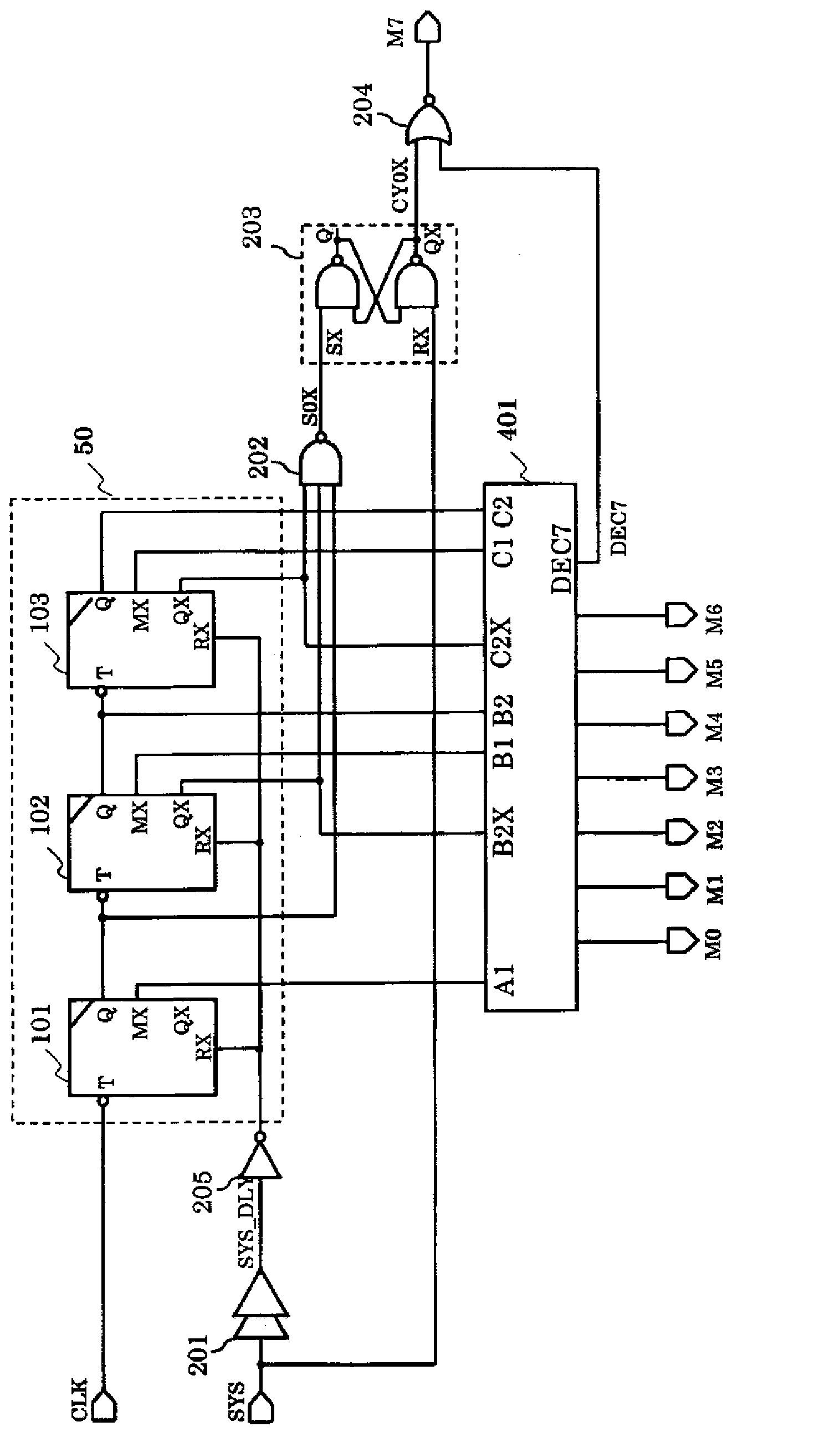
[0019] figure 1 It is a circuit diagram showing the timing generation circuit of the first embodiment.
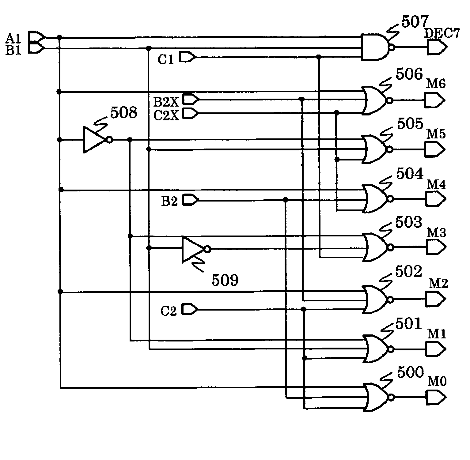
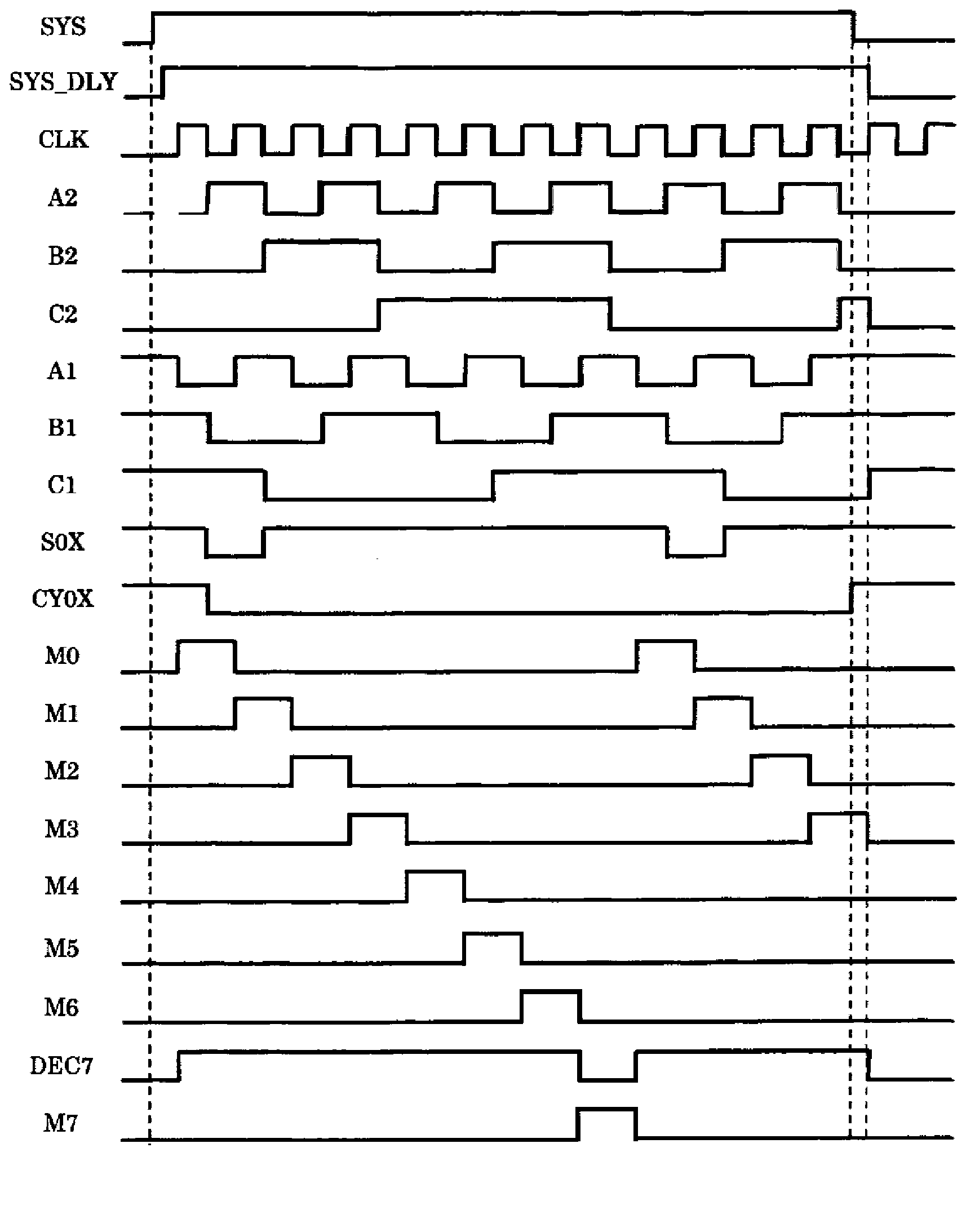
[0020] The timing generating circuit of the first embodiment includes: a 3-bit binary counter 50 composed of three T flip-flop circuits 101 to 103, a delay circuit 201, a 3NAND circuit 202, an RS latch circuit 203, a 2NOR circuit 204, and an inverter circuit. 205 and decoding circuit 401.
[0021] The clock signal input terminal CLK is connected to the input terminal of the binary counter 50 . The input terminal SYS is connected to the reset terminal of the binary counter 50 and the terminal RX of the RS latch circuit 203 via the delay circuit 201 and the inverter circuit 205 . The reset terminal of the binary counter 50 is commonly connected to the reset terminals RX of the T flip-flop circuits 101 to 103 . The output terminal of the binary counter 50 is connected to the decoding circuit 401 and the 3NAND circuit 202 . The output terminal of the 3NAND circuit 202 is c...
no. 2 Embodiment approach
[0030] In the first embodiment, eight types of output pulses with different timings are generated by a binary counter composed of a 3-bit T flip-flop circuit and a decoding circuit composed of 3NAND and 3NOR, but the number of output pulses that can be generated is not limited to 8 types. For example, by adding a D flip-flop circuit to the first embodiment, nine types of output pulses with different timings can be generated.
[0031] First, the configuration of the timing generating circuit of the second embodiment will be described. Figure 4 A circuit diagram of the timing generating circuit of the second embodiment is shown.
[0032] The timing generating circuit of the second embodiment includes: a binary counter 50, a delay circuit 201, a 3NAND circuit 202, an RS latch circuit 203, a 2NOR circuit 301, a 3NOR circuit 302, a D flip-flop circuit 303, a 3NOR circuit 304, and an inverting circuit 305. , 306 and decoding circuit 401.
[0033] The clock signal input terminal C...
PUM
 Abstract
Description
Claims
Application Information
 - Generate Ideas
- Intellectual Property
- Life Sciences
- Materials
- Tech Scout
- Unparalleled Data Quality
- Higher Quality Content
- 60% Fewer Hallucinations
Browse by: Latest US Patents, China's latest patents, Technical Efficacy Thesaurus, Application Domain, Technology Topic, Popular Technical Reports.
© 2025 PatSnap. All rights reserved.Legal|Privacy policy|Modern Slavery Act Transparency Statement|Sitemap|About US| Contact US: help@patsnap.com