

Cavity heating device
A heating device and chamber technology, applied in the direction of discharge tubes, electrical components, circuits, etc., can solve the problems of uneven chip temperature, inconsistent surface etching rate, uneven plasma, etc., and meet the requirements of maintaining vacuum. The effect of avoiding unevenness
- Summary
- Abstract
- Description
- Claims
- Application Information
AI Technical Summary
Problems solved by technology
Method used
Image

Examples
Embodiment 1
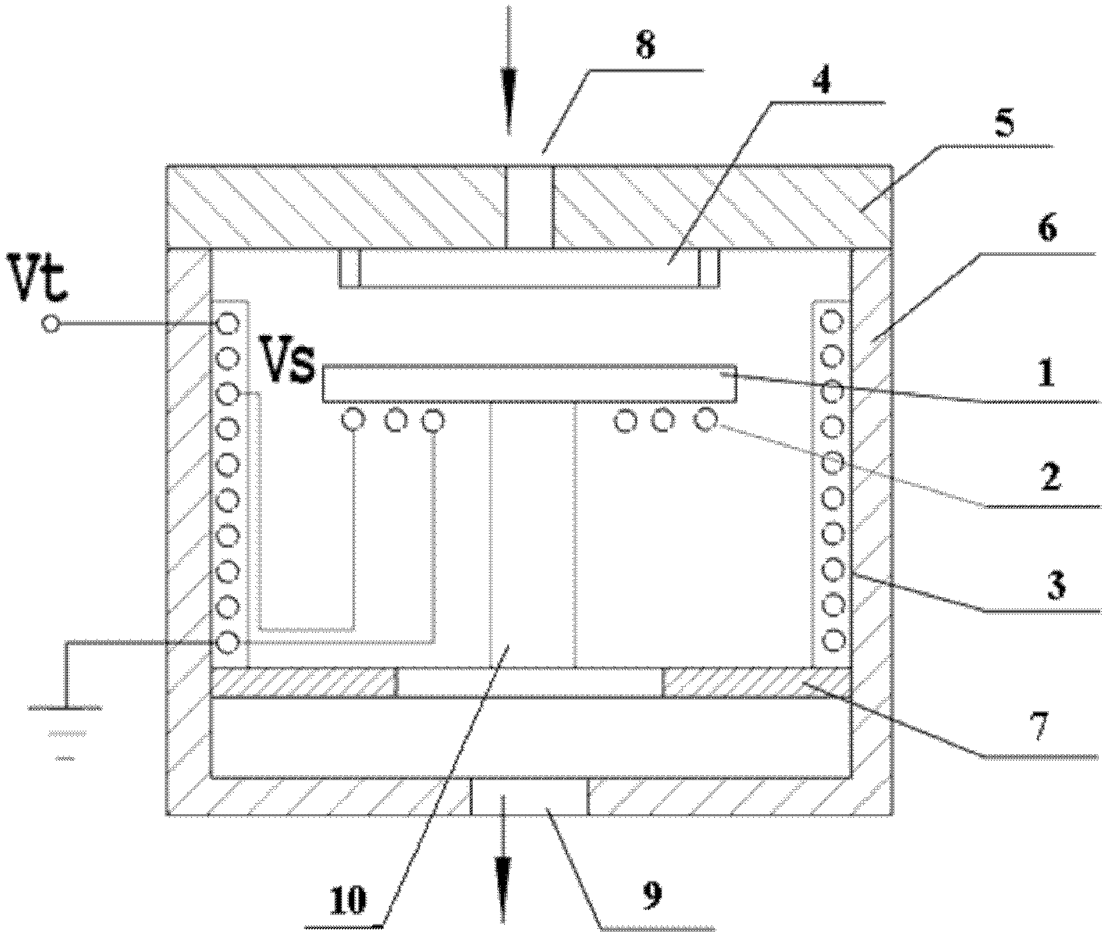
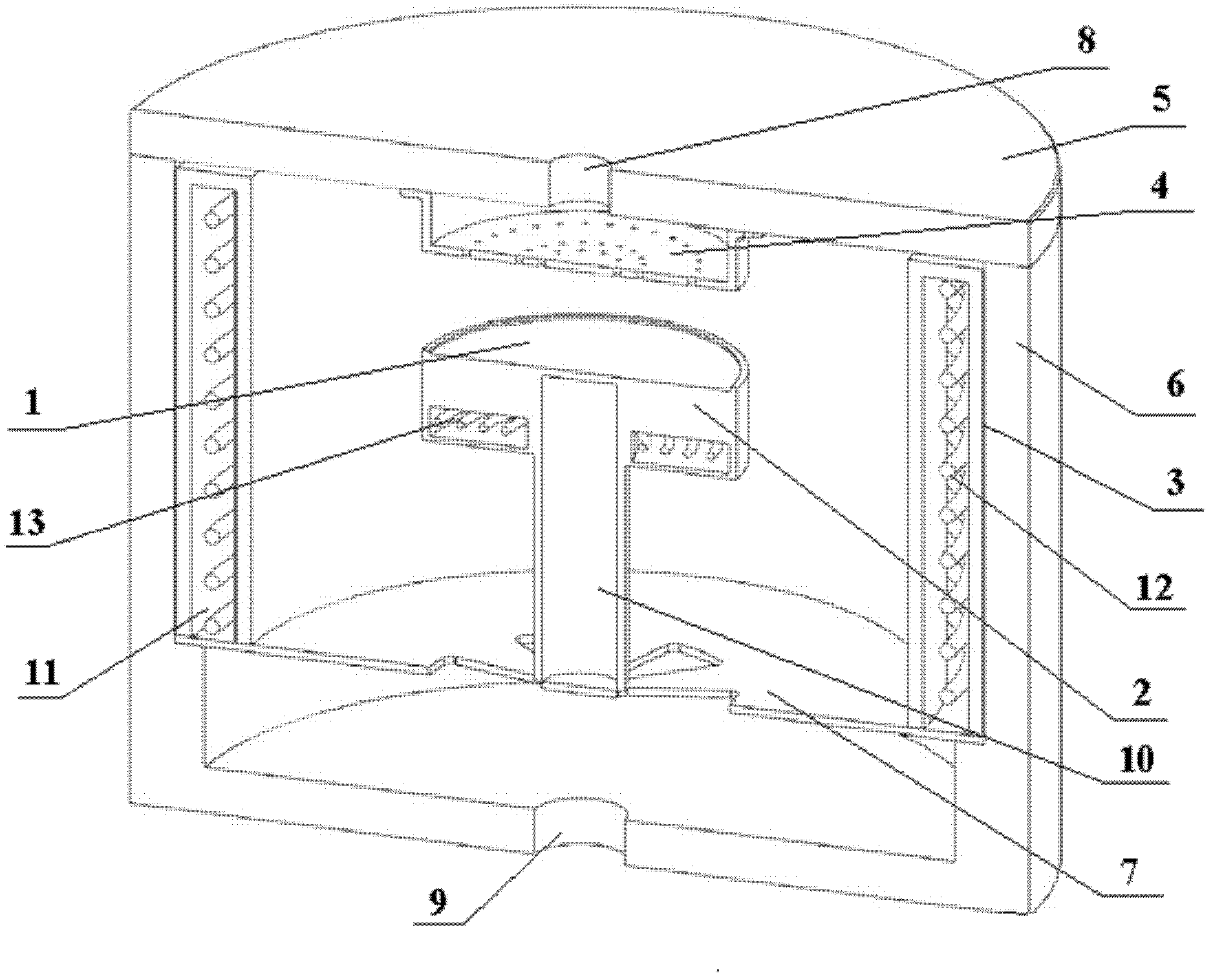
[0038] combine figure 1 , figure 2 As shown, the embodiment of the present invention provides a chamber heating device, including a slide table 1, a slide table heating structure 2, a chamber wall heating structure 3, an upper electrode 4, a chamber upper cover 5, and a reaction chamber as 6. Support plate 7, upper air inlet 8, lower air inlet 9 and support ring 10. Wherein, the slide table 1 is set at the center of the chamber wall heating structure 3 . The chamber wall heating structure 3 is installed on the inner wall of the reaction chamber 6 . The heating structure 2 of the loading table is arranged at the bottom of the loading table. The upper air inlet 8 is arranged on the upper cover 5 of the chamber. The upper electrode 4 is connected with the upper cover 5 of the chamber. The support plate 7 is fixed on the bottom of the chamber wall heating structure 3 and connected with the slide table 1 through the support ring 10 .
[0039] Wherein, the chamber wall heatin...
Embodiment 2
[0045]The difference between this embodiment and Embodiment 1 is that, in the chamber wall heating structure, the first heating coil 12 consists of 100 turns. The tube diameter of the first heating coil 12 is 200 mm, the diameter is 10000 mm, and the helical pitch is 1000 mm. The distance from the tube wall of the first heating coil to the lining wall in the chamber is 10mm. The distance between the outer wall of the liner 11 in the chamber and the inner wall of the reaction chamber 6 is 20mm. The thickness of the inner and outer walls of the bushing 11 in the chamber is 30 mm, made of molybdenum. The diameter of the inner wall of the liner 11 in the chamber is 5000mm. The lead-out electrode voltage Vt is 2000V, and the heating power Pt is 5000W.
[0046] In the loading stage heating structure 2 , the number of turns of the second heating coil 13 is 5 turns. The pipe diameter of the second heating coil 13 is 5 mm, the diameter of the innermost coil of the second heating co...
Embodiment 3
[0049] The difference between this embodiment and Embodiment 1 is that, in the chamber wall heating structure, the first heating coil 12 consists of 25 turns. The tube diameter of the first heating coil 12 is 100 mm, the diameter is 5000 mm, and the helical pitch is 500 mm. The distance from the wall of the first heating coil 12 to the lining wall in the chamber is 5 mm. The distance between the outer wall of the liner 11 in the chamber and the inner wall of the reaction chamber 6 is 10 mm. The inner and outer walls of the bushing 11 in the chamber have a thickness of 15mm and are made of SiC material. The diameter of the inner wall of the lining 11 in the chamber is 2500mm. The lead-out electrode voltage Vt is 1000V, and the heating power Pt is 5000W.
[0050] In the heating structure of the loading stage, the second heating coil 13 consists of 25 turns. The pipe diameter of the second heating coil 13 is 50 mm, the diameter of the outermost coil of the second heating coil...
PUM
 Abstract
Description
Claims
Application Information