Method for realizing high-trapping-light nanostructure single-face texture surface making

A nano-structured, single-sided texturing technology, applied in chemical instruments and methods, final product manufacturing, sustainable manufacturing/processing, etc. effect on large-scale applications

Inactive Publication Date: 2013-07-24
INST OF MICROELECTRONICS CHINESE ACAD OF SCI
View PDF3 Cites 15 Cited by
  • Summary
  • Abstract
  • Description
  • Claims
  • Application Information

AI Technical Summary

Problems solved by technology

[0003] At present, the surface reflectance of traditional crystalline silicon solar cells reaches about 12%, and the utilization rate of light is not very high.

Method used


Image

  • Method for realizing high-trapping-light nanostructure single-face texture surface making
  • Method for realizing high-trapping-light nanostructure single-face texture surface making
  • Method for realizing high-trapping-light nanostructure single-face texture surface making

Examples


Embodiment Construction

[0029] In order to make the object, technical solution and advantages of the present invention clearer, the present invention will be described in further detail below in conjunction with specific embodiments and with reference to the accompanying drawings.

[0030] In order to further explain the technical means and effects that the present invention adopts to achieve the intended purpose of the invention, below in conjunction with the accompanying drawings and preferred embodiments, the specific implementation method, The structure, characteristics and functions thereof are detailed as follows:

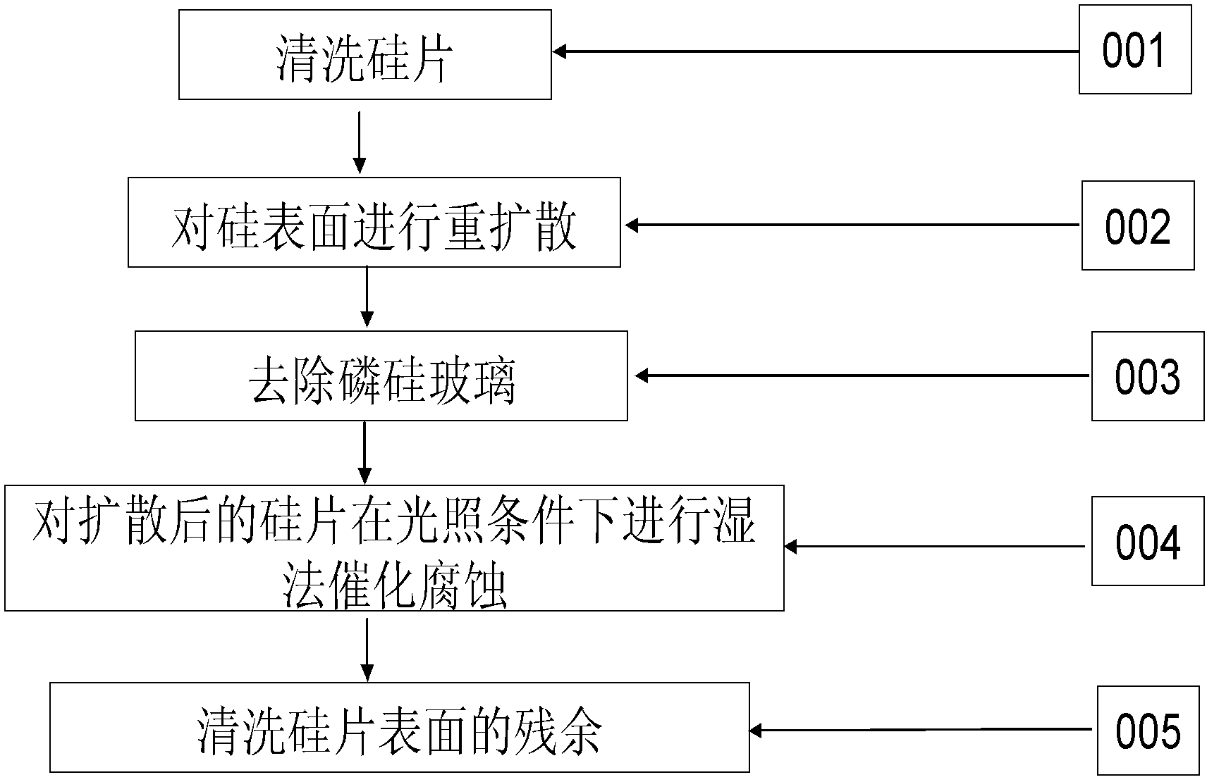
[0031] Such as figure 1 as shown, figure 1 It is a flowchart of a method for realizing high-light-trapping nanostructure single-sided texturing according to an embodiment of the present invention, and the method includes the following steps:

[0032] Step 001, cleaning the silicon wafer by RCA method;

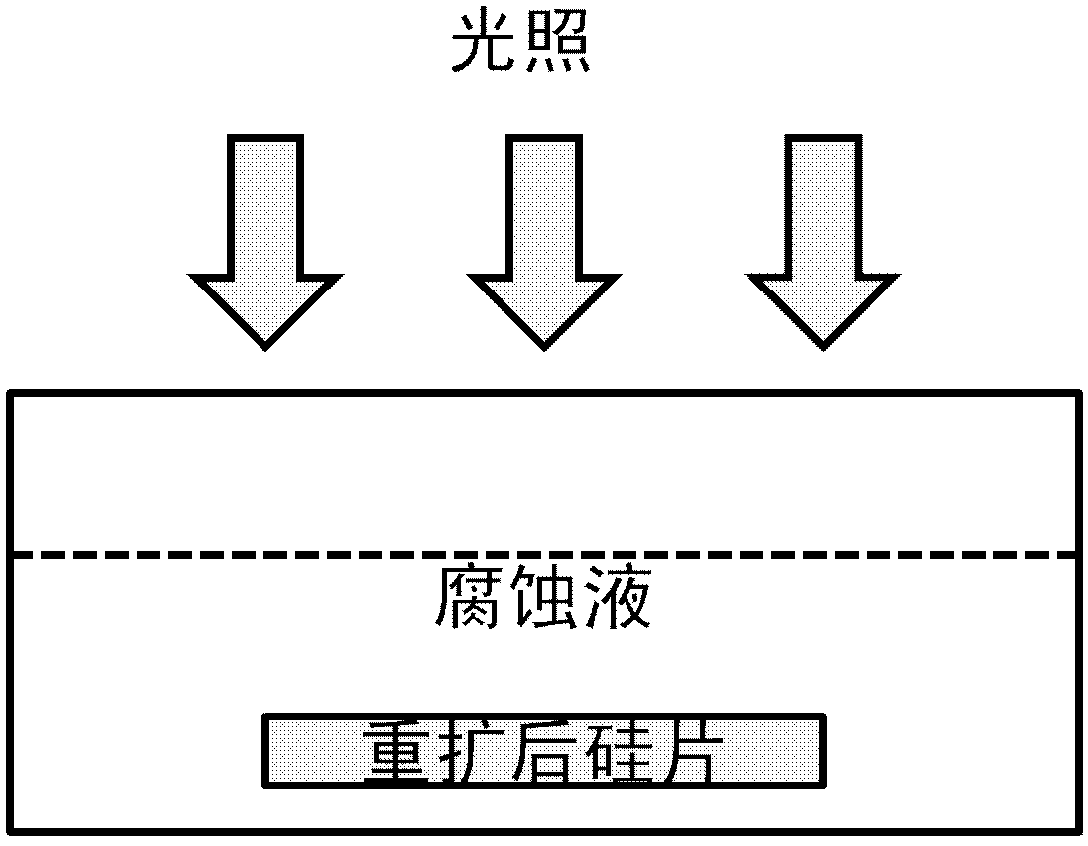
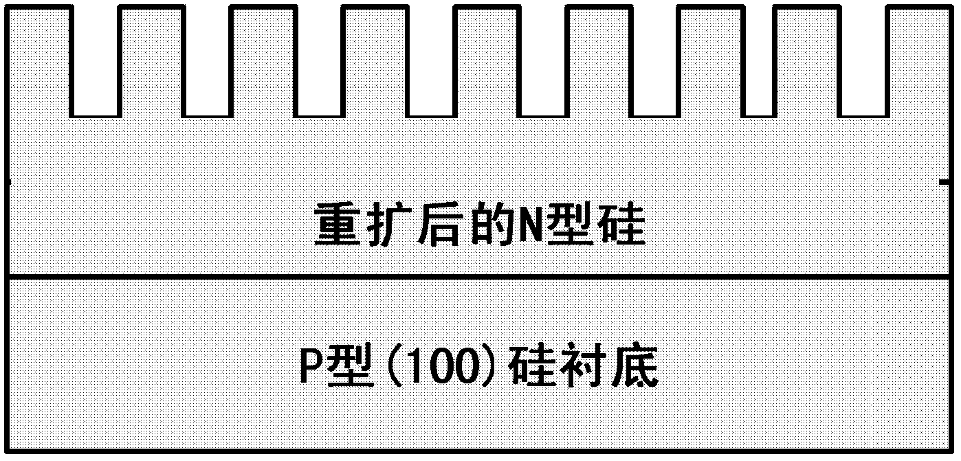
[0033] Step 002, performing re-diffusion on the surface of the silicon wafer;...


PUM


Abstract

The invention discloses a method for realizing high-trapping-light nanostructure single-face texture surface making. The method comprises the steps: cleaning a silicon wafer; conducting re-spreading to the surface of the silicon wafer; removing residues on the surface of the silicon wafer which is re-spread; coating TiO2 of a nanostructure on the surface of the silicon wafer or depositing Ti on the surface of the silicon wafer, and rapidly annealing; conducting wet etching on the silicon wafer to form the nanostructure; and removing oxide and titanium ions which are not completely reacted on the surface of the silicon wafer. Compared with the prior art, the method is adopted to prepare the high-trapping-light nanostructure, only technology sequence is changed, and under the premise that key equipment is not increased, only one light source needs to be added or only sun light needs to be led in so that the purpose of single-face texture surface making can be achieved. The nanostructure has a good light trapping effect. Besides, the method is simple in process step, and suitable for mass production.

Description

technical field [0001] The invention relates to the technical field of preparation of silicon-based high-efficiency solar cells, in particular to a method for realizing single-sided texturing of high-light-trapping nanostructures. On the basis of high light-trapping surface, there is also the effect of single-sided texturing to further improve Light trapping effect on the surface of solar cells. Background technique [0002] The solar energy received by the earth every day is equivalent to 200 times the total energy consumed by the whole world in one year, and the energy emitted by the sun every second is approximately equivalent to all the heat released when 130 million tons of standard coal are completely burned. Solar energy and its converted wind and ocean energy are the main research focus of clean energy today. Solar cells are an important renewable energy source, which can be used as an independent energy source, and can also be connected to the grid for power genera...

Claims


Application Information

Patent Timeline
Patent Type & Authority Applications(China)
IPC IPC(8): H01L31/18C30B33/10
CPCY02P70/50
Inventor 贾锐林阳陈晨金智刘新宇
Owner INST OF MICROELECTRONICS CHINESE ACAD OF SCI
Why Eureka
Try Eureka