Mounting structure for circuit component and method for mounting circuit component

A technology of circuit components and mounting structures, which is applied to electrical components, printed circuits, printed circuits, etc., and can solve problems such as large vibration of circuit components and easy vibration of circuit components

Inactive Publication Date: 2013-07-24
PANASONIC CORP
View PDF8 Cites 4 Cited by
  • Summary
  • Abstract
  • Description
  • Claims
  • Application Information

AI Technical Summary

Problems solved by technology

[0010] Furthermore, in a plasma display device with a larger screen size, due to the increase in the size of the plasma display device itself or the increase in the size of the circuit board, it becomes more likely to be affected by vibrations generated outside the plasma display device. As a result, a new problem arises: The circuit components of the substrate are prone to vibration
[0011] In particular, in a plasma display device with a built-in speaker, vibration tends to occur in circuit members as the size increases.

Method used


Image

  • Mounting structure for circuit component and method for mounting circuit component
  • Mounting structure for circuit component and method for mounting circuit component
  • Mounting structure for circuit component and method for mounting circuit component

Examples


Embodiment approach 1

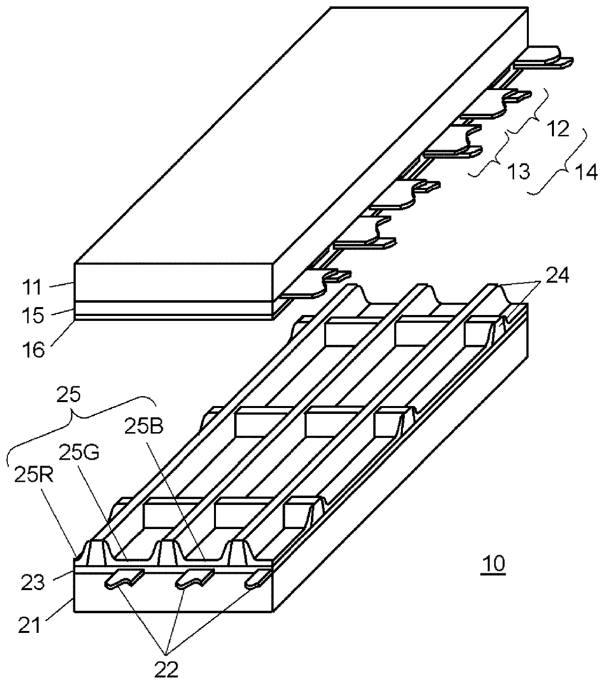
[0041] figure 1 It is an exploded perspective view showing the configuration of panel 10 employed in the plasma display device according to Embodiment 1 of the present invention.

[0042] A plurality of display electrode pairs 14 including scan electrodes 12 and sustain electrodes 13 are formed on front substrate 11 made of glass. Furthermore, dielectric layer 15 is formed so as to cover scan electrodes 12 and sustain electrodes 13 , and protective layer 16 is formed on dielectric layer 15 .

[0043]The protective layer 16 is effective as a panel material in order to reduce the discharge start voltage in the discharge cell, and has a large secondary electron emission coefficient and excellent durability when neon (Ne) and xenon (Xe) gases are enclosed. Made of a material mainly composed of magnesium oxide (MgO).

[0044] The protective layer 16 may consist of one layer, or may consist of several layers. In addition, a structure in which particles exist on a layer may be use...

Embodiment approach 2

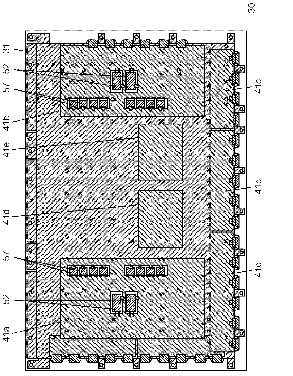
[0092] Figure 5A It is a plan view showing an example of hole portion 42 provided in circuit board 41 of plasma display device 30 according to Embodiment 2 of the present invention.

[0093] Figure 5B It is a plan view schematically showing an example of a mounting structure in which electrolytic capacitor 52 is mounted on circuit board 41 of plasma display device 30 in Embodiment 2 of the present invention.

[0094] Such as Figure 5A As shown, the circuit board 41 has a hole 42 , a through hole 43 , and a protrusion 45 .

[0095] The hole portion 42 is provided in the circuit board 41 to have a size larger than the external size of the main body portion 52 a excluding the lead wire 53 of the electrolytic capacitor 52 mounted on the circuit board 41 .

[0096] A through-hole 43 is provided in the circuit board 41 for insertion of the lead wire 53 of the electrolytic capacitor 52 .

[0097] The convex part 45 is provided on one side of the hole part 42, and has a shape w...

Embodiment approach 3

[0111] Figure 6A It is a plan view showing an example of notch portion 62 provided in circuit board 61 of plasma display device 30 in Embodiment 3 of the present invention.

[0112] Figure 6B It is a plan view schematically showing an example of a mounting structure in which electrolytic capacitor 52 is mounted on circuit board 61 of plasma display device 30 in Embodiment 3 of the present invention.

[0113] Such as Figure 6A As shown, in Embodiment 3, the circuit board 61 has the notch 62 , the through hole 63 , and the protrusion 64 .

[0114] At the corners of the circuit board 61 , cutouts 62 are provided on the circuit board 41 with dimensions larger than the external dimensions of the main body portion 52 a of the electrolytic capacitor 52 mounted on the circuit board 61 except the lead wire 53 .

[0115] In addition, although the four sides of the hole 42 shown in Embodiment 1 and Embodiment 2 are blocked by the circuit board 41, since the notch 62 in this embodim...


PUM


Abstract

In the present invention, comparatively large circuit components such as electrolytic capacitors and film capacitors are mounted on a circuit board with the height of the circuit components that protrude above the circuit board controlled while preventing noise from arising because of contact with the circuit board. To do so, the circuit board has hole parts or cutouts disposed in the main body parts for circuit components mounted on the circuit board and protruding parts having a shape that protrudes from one side or a plurality of sides of the hole parts or cutouts. Furthermore, the circuit components are disposed on the circuit board in a state where the main body parts of the circuit components pass through the hole parts or cutout parts and a state in which the main body parts of the circuit components do not come into contact with the circuit board except at the protruding parts. Furthermore, to maintain these states, the protruding parts and the main body parts of the circuit components are attached by fixing members provided on the protruding parts and the circuit components affixed to the circuit board.

Description

technical field [0001] The present invention relates to a circuit member mounting structure and a circuit member mounting method for mounting on a circuit board used in electrical equipment such as a plasma display device, for example. Background technique [0002] In a representative AC surface discharge panel as a plasma display panel (hereinafter abbreviated as "panel"), a plurality of discharge cells are formed between a front substrate and a rear substrate that are arranged to face each other. In the front substrate, a plurality of display electrode pairs are formed parallel to each other on the glass substrate on the front side, and the display electrode pairs are composed of a pair of scan electrodes and sustain electrodes. Furthermore, a dielectric layer and a protective layer are formed so as to cover these display electrode pairs. [0003] In the rear substrate, a plurality of parallel data electrodes are formed on a glass substrate on the rear side, a dielectric ...

Claims


Application Information

Patent Timeline
Patent Type & Authority Applications(China)
IPC IPC(8): H05K1/18
CPCH05K2201/2036H05K3/3447H05K1/181H05K3/301H05K2201/09063H05K2203/167H05K1/184H05K2201/2045Y10T29/4913H05K1/18
Inventor 岩崎友哉金野裕则
Owner PANASONIC CORP
Why Eureka
Try Eureka