Apparatus for realizing multi-chip Nandflash storage and read based on FPGA

A memory bank, memory array technology, applied in information storage, static memory, read-only memory, etc., can solve problems such as limited pins, inability to expand bandwidth, storage errors, etc., to achieve stable physical properties, capacity improvement, The effect of speed increase

Inactive Publication Date: 2013-07-31
INST OF ACOUSTICS CHINESE ACAD OF SCI
View PDF5 Cites 5 Cited by
  • Summary
  • Abstract
  • Description
  • Claims
  • Application Information

AI Technical Summary

Problems solved by technology

[0006] Due to the unstable physical properties of storage devices, existing solutions are prone to storage errors. Many storage controllers use DSP, single-chip microcomputers, and ARMs. It is difficult to design a high-speed storage solution for the multi-channel data storage of this system by the method; the main disadvantages of the existing method are listed in detail below:

Method used


Image

  • Apparatus for realizing multi-chip Nandflash storage and read based on FPGA
  • Apparatus for realizing multi-chip Nandflash storage and read based on FPGA
  • Apparatus for realizing multi-chip Nandflash storage and read based on FPGA

Examples


Embodiment Construction

[0030] In order to make the object, technical solution and advantages of the present invention clearer, the present invention will be further described in detail below in conjunction with the accompanying drawings and embodiments. It should be understood that the specific embodiments described here are only used to explain the present invention, not to limit the present invention.

[0031] Below in conjunction with accompanying drawing, the present invention is described in detail, and the detailed structure of the present invention is as follows: Figure II :

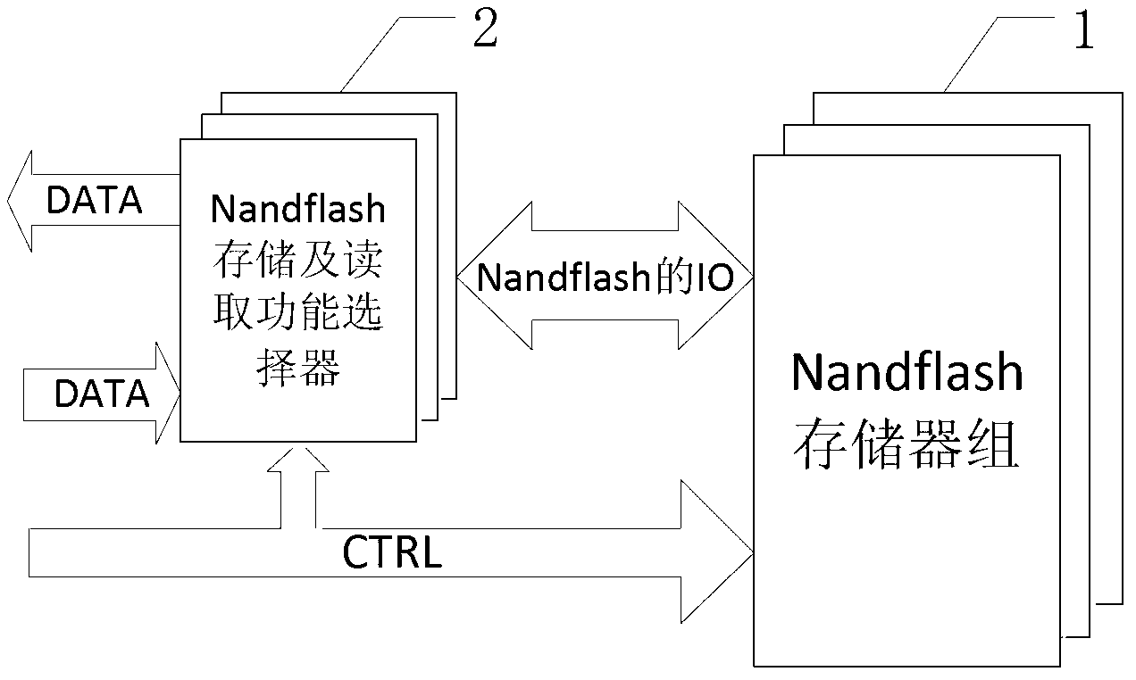
[0032] see figure 2 , Nandflash storage and read function selector 2 and Nandflash memory bank 1 are core parts of the present invention, need to be introduced.

[0033] The specific structure is described as follows:

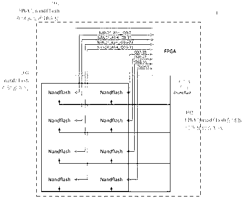
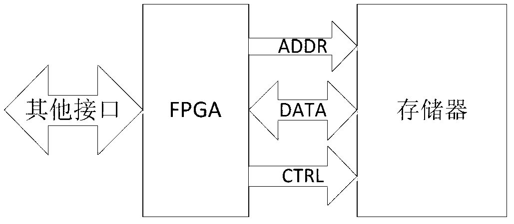
[0034] 1. Nandflash memory group, this part is the Nandflash memory group, including the hardware connection between FPGA and Nandflash memory group, including the hardware connection of IO line and...


PUM


Abstract

The invention discloses an apparatus for realizing multi-chip Nandflash storage and read based on FPGA. The apparatus comprises an Nandflash memory group, wherein the Nandflash memory group includes a memory array composed of a plurality of Nandflash chips and is used for storing the ADC sampling data output to Nandflash by FPGA; and an Nandflash storage and read function selector used for data reading and writing, and ID information erasing and reading of the Nandflash memory group. The above technical scheme allows the quantity of pins to be increased by times, and the data transmission bandwidth in the physical layer to be expanded, so the transmission rate is greatly raised, and the FPGA program exploitation difficulty is reduced because of the only expansion in the physical layer.

Description

technical field [0001] The invention relates to the field of analog-to-digital conversion storage technology and FPGA-based development and design, in particular to the technology of using a Nandflash chip with stable physical performance to establish a reliable expandable storage mechanism. Background technique [0002] A general memory control structure such as figure 1 As shown: the interface between the memory and the FPGA is mainly divided into address lines, data lines and control lines. The advantage of this method is that it is highly operable. When reading and writing, as long as the address is given by the FPGA, the memory can be precisely controlled. [0003] But in more specific applications, such as sonar system data acquisition, it is hoped that the memory can input data accurately and stably, and the data can be played back after the sonar system is running. So choose non-volatile memory. [0004] Non-volatile memory means that the stored data will not disap...

Claims


Application Information

Patent Timeline
Patent Type & Authority Applications(China)
IPC IPC(8): G11C16/06
Inventor 马晓川鄢社锋林津丞杨力彭承彦王敏
Owner INST OF ACOUSTICS CHINESE ACAD OF SCI
Why Eureka
Try Eureka