

Two-dimensional plasma photonic crystal band gap control method
A plasma and photonic crystal technology, which is used in the control field of the band gap formation of microwave devices, and can solve the problems of high model size and distribution requirements and complex methods.
- Summary
- Abstract
- Description
- Claims
- Application Information
AI Technical Summary
Problems solved by technology
Method used
Image

Examples
Embodiment Construction
[0020] The technical solution of the present invention will be described in further detail below according to the accompanying drawings.
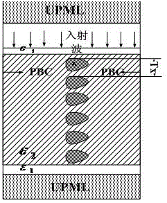
[0021] Such as figure 1 As shown, the basic flow of modeling of plasmonic photonic crystals is as follows
[0022] Step (1) Establish a rectangular solid model for a single cell using the finite-difference method in time domain. coincidence, the dielectric constant ε of the model background medium 2 Greater than 0.
[0023] Step (2) uniformly embed N identical plasma media in the background medium, and the dielectric constant of the plasma media is denoted as ε 3 .
[0024] Step (3) In the rectangular solid model of a single cell, the outer sides of the two opposite sides that have a gap with the background medium of the rectangular model are close to the opposite sides, and the UPML absorption boundary is added respectively, and the dielectric constant is filled between the absorption boundary and the background med...
PUM
| Property | Measurement | Unit |
|---|---|---|
| length | aaaaa | aaaaa |
Abstract
Description
Claims
Application Information