Thin film transistor baseplate and preparation method thereof
A technology of thin-film transistors and substrates, which is applied in the direction of electric solid-state devices, semiconductor devices, semiconductor/solid-state device components, etc., and can solve the problems that static electricity cannot be eliminated at any time and cannot be effectively eliminated
- Summary
- Abstract
- Description
- Claims
- Application Information
AI Technical Summary
Problems solved by technology
Method used
Image
Examples
preparation example Construction
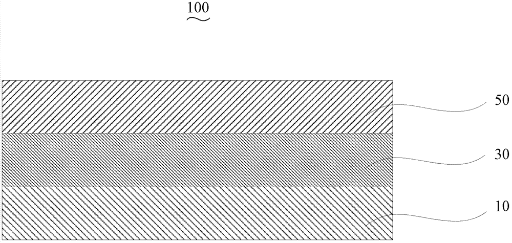
[0029] Please also see figure 2 , the preparation method of the thin film transistor substrate 100 of an embodiment, comprises the following steps:
[0030] Step S110 , forming a protection layer 30 on the substrate 10 , the material of the protection layer 30 is silicon dioxide.
[0031] In this embodiment, the substrate 10 is pretreated to remove dirt and dust on the surface of the substrate 10 before forming the protective layer 30 . The pretreatment steps are as follows: first clean the base 10 with pure water, blow off the water on the surface of the base 10 with cold wind, then blow the base 10 with hot air to dry, and then perform quality inspection on the dried base 10, if the base 10 is If the surface is free of dirt and scratches, the substrate 10 is qualified and can be prepared for coating.
[0032] In this embodiment, the protective layer 30 is formed by vacuum magnetron sputtering, and the process parameters of the vacuum magnetron sputtering protective layer ...
Embodiment 1
[0038] The substrate 10 is pretreated to remove dirt and dust on the surface of the substrate 10 . The pretreatment steps are as follows: first clean the base 10 with pure water, blow off the water on the surface of the base 10 with cold wind, then blow the base 10 with hot air to dry, and then check the quality of the dried base 10, if the base 10 is If the surface is free of dirt and scratches, the substrate 10 is qualified and can be prepared for coating.
[0039] Vacuum sputtering of SiO on the substrate 10 using a WG vacuum magnetron sputtering coating machine 2 The film forms the protective layer 30 . The target material is polysilicon, and there are two target materials in total. During the vacuum sputtering process, the heating temperature of the substrate 10 is 50°C, the heating time of the substrate 10 is 450S, the running speed of the substrate 10 is 13.3mm / S, the coating time is 150S, and the vacuum degree of the coating chamber is 3.5×10 -1 Pa, the total air pr...
Embodiment 2
[0042] The substrate 10 is pretreated to remove dirt and dust on the surface of the substrate 10 . The pretreatment steps are as follows: first clean the base 10 with pure water, blow off the water on the surface of the base 10 with cold wind, then blow the base 10 with hot air to dry, and then perform quality inspection on the dried base 10, if the base 10 is If the surface is free of dirt and scratches, the substrate 10 is qualified and can be prepared for coating.
[0043] Vacuum sputtering of SiO on the substrate 10 using a WG vacuum magnetron sputtering coating machine 2 The film forms the protective layer 30 . The target material is polysilicon, and there are two target materials in total. During the vacuum sputtering process, the heating temperature of the substrate 10 is 80°C, the heating time of the substrate 10 is 270S, the running speed of the substrate 10 is 22.2mm / S, the coating time is 90S, and the vacuum degree of the coating chamber is 2.5×10 -1 Pa, the tota...
PUM
| Property | Measurement | Unit |
|---|---|---|
| Thickness | aaaaa | aaaaa |
| Thickness | aaaaa | aaaaa |
| Thickness | aaaaa | aaaaa |
Abstract
Description
Claims
Application Information

