A linearly doped graphene field effect transistor with a dual-material gate

A field-effect transistor and dual-material technology, applied in electrical components, circuits, semiconductor devices, etc., can solve problems such as device performance degradation, and achieve the effects of small threshold voltage drift, large threshold voltage, and good gate control ability

Active Publication Date: 2016-08-17
NANJING UNIV OF POSTS & TELECOMM INST AT NANJING CO LTD
View PDF6 Cites 0 Cited by
  • Summary
  • Abstract
  • Description
  • Claims
  • Application Information

AI Technical Summary

Problems solved by technology

[0005] Technical problem: The purpose of this invention is to solve the problem of device performance degradation caused by short channel effect and other series of side effects of traditional nano-devices, and to provide a dual-material heterogeneous gate field effect transistor, so that the device can suppress heat-carrying current Sub-effects are also enhanced

Method used


Image

  • A linearly doped graphene field effect transistor with a dual-material gate
  • A linearly doped graphene field effect transistor with a dual-material gate
  • A linearly doped graphene field effect transistor with a dual-material gate

Examples


Embodiment Construction

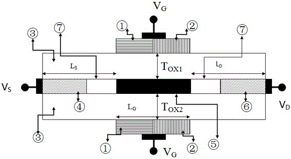
[0014] The field effect transistor has a sheet-like structure as a whole, and the source and drain are n-type heavily doped graphene nanoribbons;

[0015] The two ends of the graphene field effect tube are respectively provided with a source and a drain, and the source and drain regions are heavily doped with N-type with the same parameters; the middle part of the graphene field effect tube is a channel area, and the channel area is not doped. miscellaneous;

[0016] Viewed from the direction of the channel, the gate is located in the middle of the channel region of the graphene field effect transistor, and its length is equal to the length of the channel region.

[0017] The heterogeneous gate is composed of two conductive metal materials with different work functions. The two materials are distributed sequentially along the channel direction, and their work functions are distributed as follows: the work function on the side near the source region is greater than that on the ...


PUM


Abstract

The invention discloses a graphene field-effect transistor linearly doped with a bi-material gate. On the basis of a quantum mechanics nonequilibrium green function theoretical framework, a transport model suitable for the graphene field-effect transistor is built through self-consistent solution Poisson and Schrodinger equation, and further, the influence of a homogenous-material gate and a bi-material heterogeneous gate strategy on electrical properties of the GNRFET (graphene nanoribbon field-effect transistor) is analyzed and calculated by the model. Compared with the electrical properties, such as the output characteristic, the transfer characteristic, the switching current ratio and the like, of the field-effect transistor adopting the bi-material gate, the field-effect transistor adopting a bi-material heterogeneous gate underlap linear doped strategic structure has the larger switching current ratio, and smaller subthreshold amplitude and threshold voltage drift, and namely, the bi-material heterogeneous gate underlap linear doping has a better gate-control capacity, so that a short-channel effect, a band-to-band tunneling effect and a hot carrier effect can be restrained effectively.

Description

technical field [0001] The invention relates to the field of graphene field effect transistors, in particular to a heterogeneous grid structure of graphene field effect transistors. Background technique [0002] In recent years, the appearance of graphene has stirred up huge waves in the scientific community, and it is considered to be one of the most promising carbon nanomaterials in the future due to its superior properties. Graphene has high electron mobility and high conductivity. Transistors made of graphene are not only small in size, low in power consumption, and low in requirements for the working environment, but also easy to design into various structures. However, since graphene is a zero-bandgap material and its Fermi energy is distributed linearly, it is not suitable for direct application in transistors. However, the band gap can be generated by cutting graphene into strips in a certain direction [HAN M Y, OZYILMAZ B, KIM P, et al. Energy band-gap engineering ...

Claims


Application Information

Patent Timeline
Patent Type & Authority Patents(China)
IPC IPC(8): H01L29/78H01L29/49H01L29/36
Inventor 王伟王燕闫帅军
Owner NANJING UNIV OF POSTS & TELECOMM INST AT NANJING CO LTD
Why Eureka
Try Eureka