Method for manufacturing silicon carbide semiconductor device and silicon carbide semiconductor device
A semiconductor and silicon carbide technology, which is applied in the field of manufacturing silicon carbide semiconductor devices, can solve problems such as the charge compensation structure of silicon carbide semiconductor devices that are not mentioned
- Summary
- Abstract
- Description
- Claims
- Application Information
AI Technical Summary
Problems solved by technology
Method used
Image

Examples
Embodiment Construction
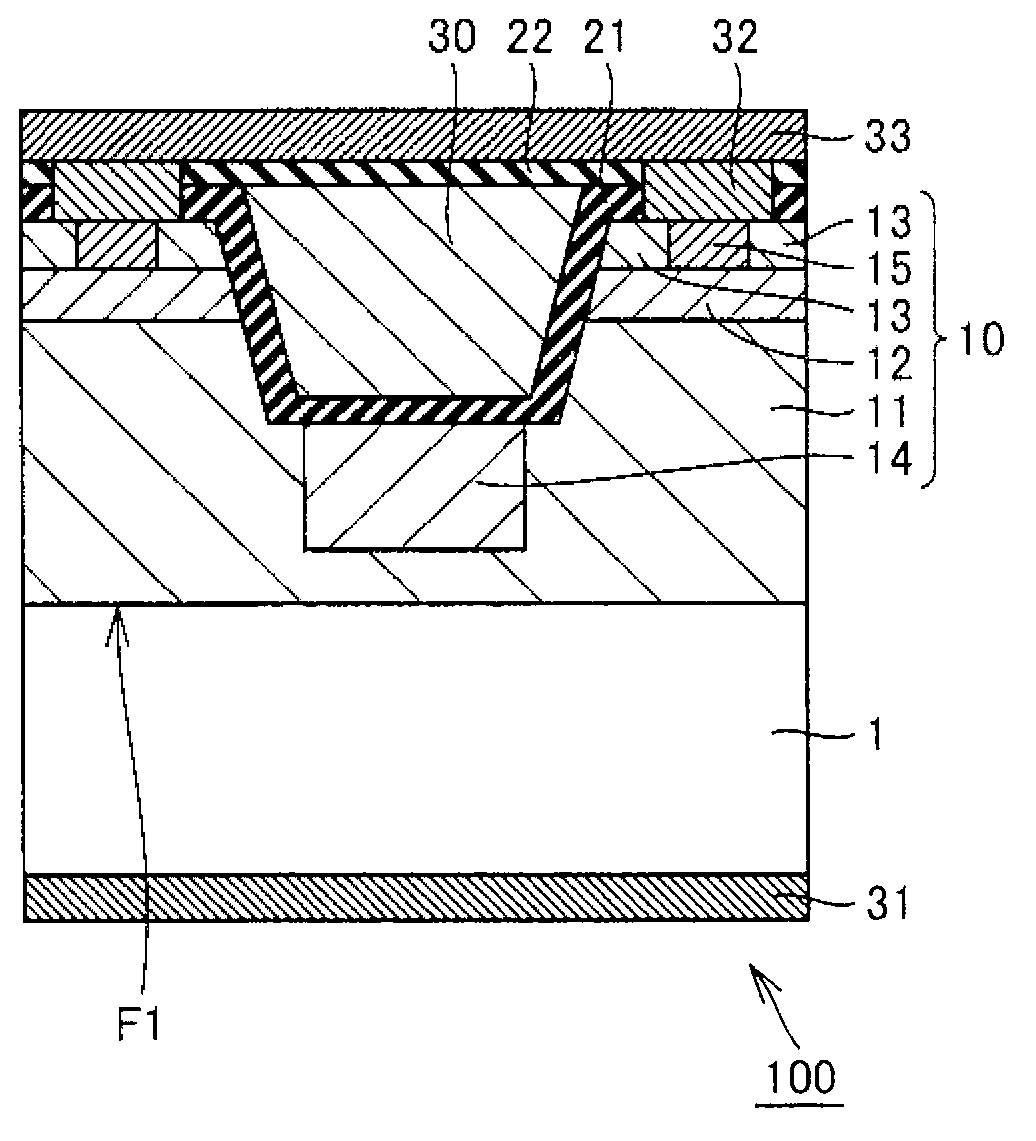
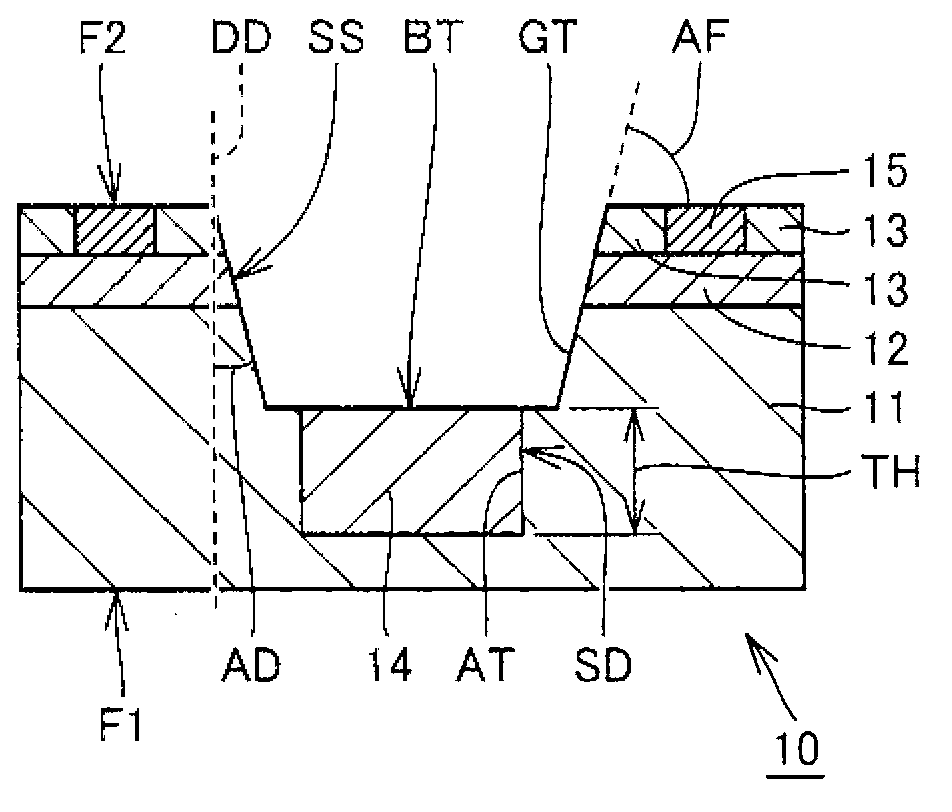
[0034] Hereinafter, an embodiment of the present invention will be described based on the drawings. In the drawings explained below, the same reference numerals are assigned to the same or corresponding elements, and the description thereof will not be repeated. As for the crystallographic representation in this specification, the specific face is represented by (), and the set of the same face is represented by {}. For negative indices, in crystallography, a bar (-) is usually assigned above the value. However, in this manual, a minus sign will be appended before the value.
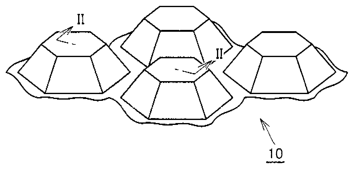
[0035] First, refer to Figure 1 to Figure 5 The structure of the MOSFET 100 (silicon carbide semiconductor device) according to the present embodiment is described.
[0036] Such as figure 1 As shown in, MOSFET 100 includes single crystal substrate 1, SiC layer 10 (silicon carbide layer), drain electrode 31 (first electrode), source electrode 32 (second electrode), gate oxide film 21 (gate insulating film)...
PUM
| Property | Measurement | Unit |
|---|---|---|
| thickness | aaaaa | aaaaa |
Abstract
Description
Claims
Application Information
 - Generate Ideas
- Intellectual Property
- Life Sciences
- Materials
- Tech Scout
- Unparalleled Data Quality
- Higher Quality Content
- 60% Fewer Hallucinations
Browse by: Latest US Patents, China's latest patents, Technical Efficacy Thesaurus, Application Domain, Technology Topic, Popular Technical Reports.
© 2025 PatSnap. All rights reserved.Legal|Privacy policy|Modern Slavery Act Transparency Statement|Sitemap|About US| Contact US: help@patsnap.com