Device and method for preparing nano imaged substrate

A technology of nano-patterning and preparation device, which is applied in the direction of photolithography process exposure device, nanotechnology, microlithography exposure equipment, etc., can solve the problems of unguaranteed uniformity and large randomness, etc.

Active Publication Date: 2013-09-04
SVG TECH GRP CO LTD +1
View PDF15 Cites 18 Cited by
  • Summary
  • Abstract
  • Description
  • Claims
  • Application Information

AI Technical Summary

Problems solved by technology

[0012] Lan Hongbo and others proposed a nanoimprint method (CN102591142B, 201210376654.5), but in practical engineering applications, there are still a series of technical problems to be solved, such as the preparation of work templates, uniformity of imprinting, mold release, and high-efficiency processes.
[0013] Patents such as 200910256023.8, 201110153487.3, and 201110330648.1 proposed the use of nanosphere coating methods to make nanostructure masks, but this method is highly random and uniformity cannot be guaranteed
[0016] In view of the above situation, there is an urgent need to develop a low-cost, high-production-efficiency nano-patterning lithography method and system to solve the engineering problems of nano-patterning production

Method used


Image

  • Device and method for preparing nano imaged substrate
  • Device and method for preparing nano imaged substrate
  • Device and method for preparing nano imaged substrate

Examples


Embodiment approach 1

[0073] In the first embodiment, it is proposed to make a photonic crystal with a pixelated structure on the substrate. A small field of view exposure spot is a pixel, which corresponds to the size of the LED chip unit. The inside of the spot is a photonic crystal structure, and the photonic crystal between the spots The structure does not necessarily need to be continuous, and the distribution of these exposure spots only needs to correspond to the positions of all LED chips on the wafer. Such as Image 6shown. The specific geometric parameters of the light spot profile, the pixel position interval and the structural parameters of the photonic crystal are determined by the engineering designer according to the specific LED parameters. The advantage of this implementation is that on a large substrate, the size and shape of a single exposure pattern is equivalent to the size of an LED chip, so there is no need to consider the continuity of the dot matrix in the spot during expo...

Embodiment approach 2

[0083] In the method described in Embodiment 1, the photonic crystal pixelated structure needs to be aligned with the subsequent process of LED production, and the splitting needs to be carried out along the grid between pixels.

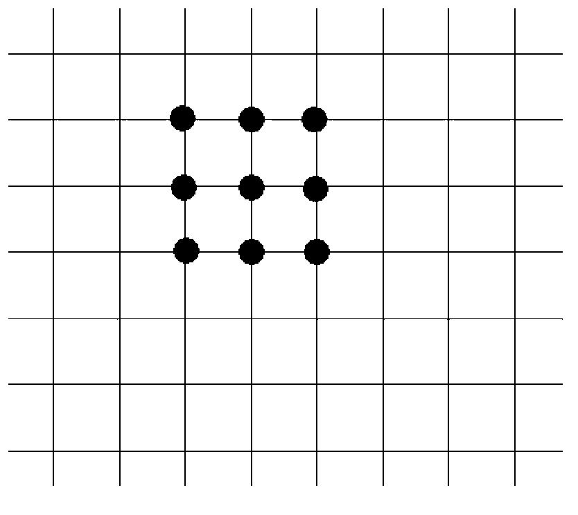
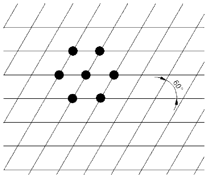
[0084] In order to optimize the manufacturing process and reduce the complexity of subsequent processes, it is proposed in the second embodiment to fabricate a continuous photonic crystal structure on the substrate. The shape of the small-field interference spot is a simple geometric shape such as a square, a rectangle, and a polygon. By giving a suitable step distance, the spots are sequentially spliced ​​to form a complete large-area continuous photonic crystal structure pattern. Such as Figure 7 As shown in , it is a schematic diagram of splicing a square spot and a regular hexagon spot.

[0085] Schematic diagram of the splicing of square spots to form a continuous nanophotonic crystal structure, such as Figure 8 shown.

[0086] Schematic di...


PUM


Abstract

The invention relates to a device and a method for preparing a nano imaged substrate. According to the preparation method, by means of the insensitivity of laser interference exposure to warping of the substrate, the defocus problem brought to a conventional imaging technology due to the warping characteristic of a sapphire substrate is solved. In the preparation device, an optical system which can modulate phase and space optical field information is designed, so that a laser interference exposure system can control sizes of interference light spots and inside dot matrix distribution, and industrial application possibility is brought to the nano imaging process of the substrate.

Description

technical field [0001] The invention relates to a method and system specially used in the field of LED nanophotonic crystal patterned substrate preparation, which is the next generation technology of the existing LED micro-patterned substrate preparation technology, and aims to optimize the patterning key in the LED process chain On the basis of the existing micro-patterned substrate technology, the luminous efficiency of LEDs is further improved, the qualified rate of patterned substrate preparation is improved, and the production cost is reduced, which will help the popularization of patterned technology in the LED industry. Background technique [0002] According to the research of the market research organization Mountain View, the global high-brightness LED market will reach a market value of US$16.2 billion by 2014, driven by demand for flat-panel TVs, mobile devices, and energy-saving lighting. Improving light extraction efficiency and reducing costs are the persisten...

Claims


Application Information

Patent Timeline
Patent Type & Authority Applications(China)
IPC IPC(8): G03F7/20B82Y40/00
Inventor 浦东林魏国军袁晓峰朱鸣朱鹏飞胡进陈林森
Owner SVG TECH GRP CO LTD
Why Eureka
Try Eureka