This helps you quickly interpret patents by identifying the three key elements:
Problems solved by technology
Method used
Benefits of technology
Problems solved by technology
However, when the panel area is large, due to the difference in the thermal expansion coefficient between the mask and the glass substrate, etc., it is difficult to ensure the alignment accuracy of the mask, so a normal display cannot be produced
In order to overcome these problems, there is a method of using a white light-emitting layer on the entire surface and installing RGB color filters (color filters) to avoid separate coating, but in this case, the light taken out is 1 / 3 of the emitted light , so in principle it has the disadvantage of increased power consumption
Method used
Image
Click on the blue label to locate the original text in one second.
Reading with bidirectional positioning of images and text.
Examples
Embodiment approach 1
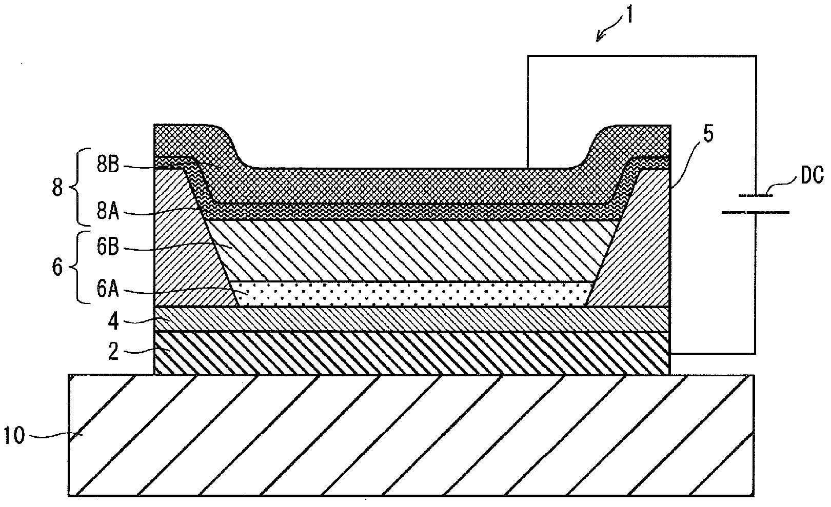
[0119] (Structure of organic EL element)
[0120] figure 1 It is a schematic cross-sectional view showing the structure of the organic EL element 1 of the first embodiment.
[0121] The organic EL element 1 is a coating type in which a functional layer is formed by coating by a wet process, and has a structure in which a hole injection layer 4 and various functional layers (here, a buffer layer 6A and a light emitting layer 6B) are placed on top of each other. Interposed between the electrode pair consisting of the anode 2 and the cathode 8 in a stacked state, the various functional layers include organic materials having predetermined functions.
[0122] Specifically, as figure 1 As shown, the organic EL element 1 is formed by stacking an anode 2, a hole injection layer 4, a buffer layer 6A, a light emitting layer 6B, and a cathode 8 (a barium layer 8A and an aluminum layer 8B) on one main surface of a substrate 10 in the following order. constituted. A power supply DC is...
Embodiment approach 2
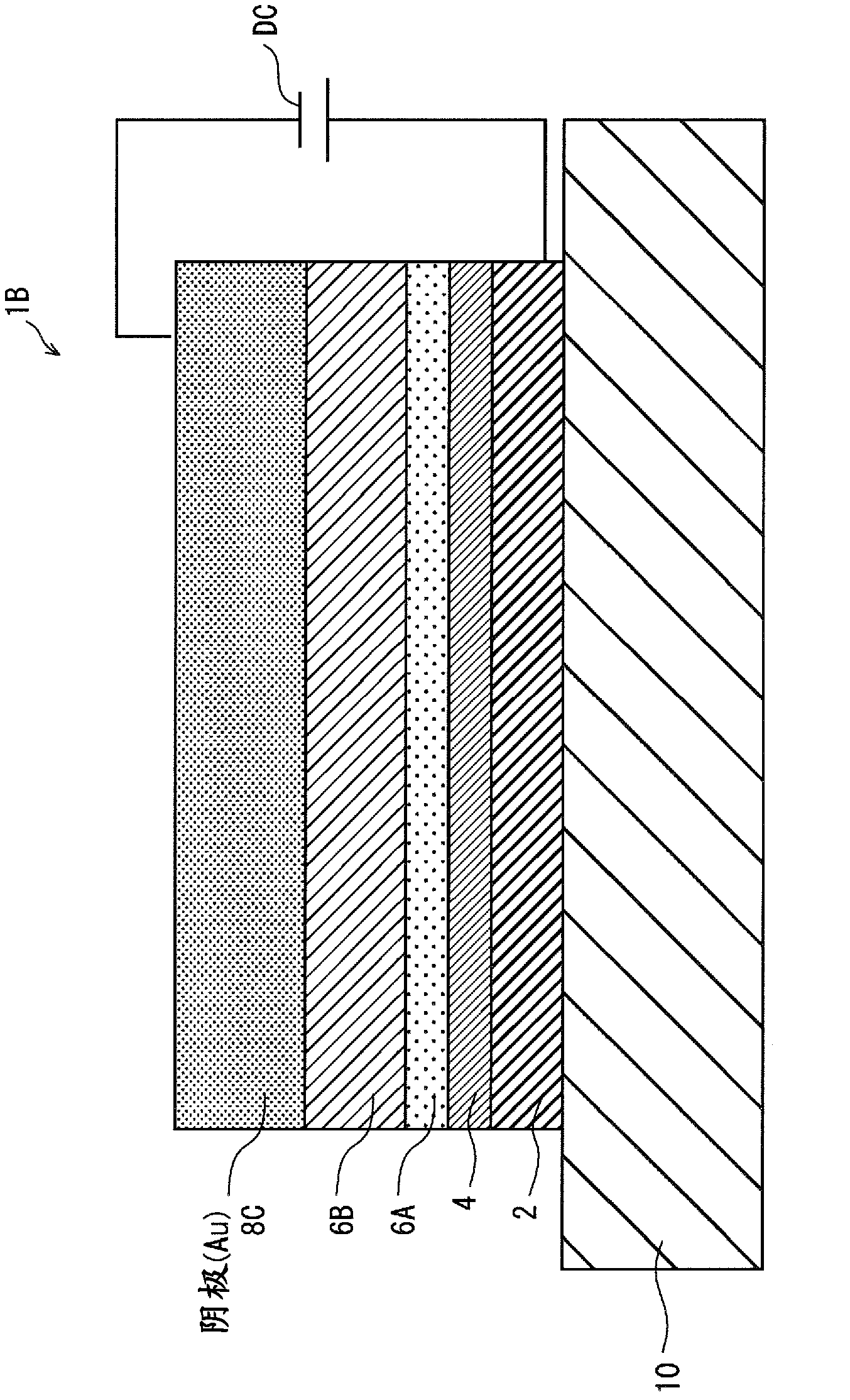
[0335]
[0336] Figure 25 (a) is a schematic cross-sectional view showing the structure of the organic EL element 1C according to the present embodiment. Figure 25 (b) is a partially enlarged view near the hole injection layer 4A.
[0337] The organic EL element 1C is, for example, a coating type in which a functional layer is formed by coating by a wet process, and has a structure in which a hole injection layer 4 and various functional layers are stacked on each other between the anode 2 and the Between the pair of electrodes constituted by the cathode 8D, the various functional layers include organic materials having predetermined functions.
[0338] Specifically, in the organic EL element 1C, an anode 2, an ITO layer 3, a hole injection layer 4A, a buffer layer 6A, a light emitting layer 6B, an electron injection layer 7, and a cathode 8D are laminated on one main surface of a substrate 10 in the following order. , Sealing layer 9 and constitute. The following descr...
PUM
Abstract
The present invention provides an organic EL element that can withstand the mass-production processes for organic EL display panels and with which high luminous efficiency can be expected with low-voltage drive because of superior hole injection efficiency. Specifically, an organic EL element (1) is formed by laminating a positive electrode (2), hole injection layer (4), buffer layer (6A), light emitting layer (6B), and negative electrode (8) in that order on one surface of a substrate (10). The hole injection layer (4) is a tungsten oxide layer with a film thickness of 2 nm or greater formed under prescribed film forming conditions, and in the electronic state thereof, the occupancy level is within a range of bond energy 1.8 - 3.6 eV lower than the lowest bond energy in the valence band. Thus, impediments to hole injection between the positive electrode (2) and the hole injection layer (4) and between the hole injection layer (4) and the buffer layer (6A) are reduced.
Description
technical field [0001] The present invention relates to an organic electroluminescence element (hereinafter referred to as "organic EL element") as an electroluminescence element, and particularly relates to a wide range of luminance for use in applications ranging from low luminance to high luminance for light source applications. Range technology for driving with low power. Background technique [0002] In recent years, research and development of various functional elements using organic semiconductors has been progressing. [0003] As a representative functional element, there is an organic EL element. The organic EL element is a current-driven light-emitting element, and has a structure in which a functional layer made of an organic material is provided between a pair of electrodes consisting of an anode and a cathode. Functional layers include light-emitting layers, buffer layers, and the like. A hole injection layer for injecting holes may be arranged between the f...
Claims
Application Information
Patent Timeline
Application Date:The date an application was filed.
Publication Date:The date a patent or application was officially published.
First Publication Date:The earliest publication date of a patent with the same application number.
Issue Date:Publication date of the patent grant document.
PCT Entry Date:The Entry date of PCT National Phase.
Estimated Expiry Date:The statutory expiry date of a patent right according to the Patent Law, and it is the longest term of protection that the patent right can achieve without the termination of the patent right due to other reasons(Term extension factor has been taken into account ).
Invalid Date:Actual expiry date is based on effective date or publication date of legal transaction data of invalid patent.
