Photoresist treatment method and preparation method of semiconductor device

A processing method and photoresist technology, which are applied in semiconductor/solid-state device manufacturing, original components for photomechanical processing, pre-treated surfaces, etc., can solve the problems of unsuitable baking temperature, deformation of photoresist 120 patterns, and baking The training time should not be too long to achieve the effect of reducing defects, ensuring line width and improving surface density

Active Publication Date: 2013-09-11
SHANGHAI HUALI MICROELECTRONICS CORP
View PDF6 Cites 0 Cited by
  • Summary
  • Abstract
  • Description
  • Claims
  • Application Information

AI Technical Summary

Problems solved by technology

[0011] However, there are still some problems that need to be solved in the existing method for preventing photoresist defects from being produced in the wet etching process: in method 1), the baking temper

Method used


Image

  • Photoresist treatment method and preparation method of semiconductor device
  • Photoresist treatment method and preparation method of semiconductor device
  • Photoresist treatment method and preparation method of semiconductor device

Examples


Embodiment Construction

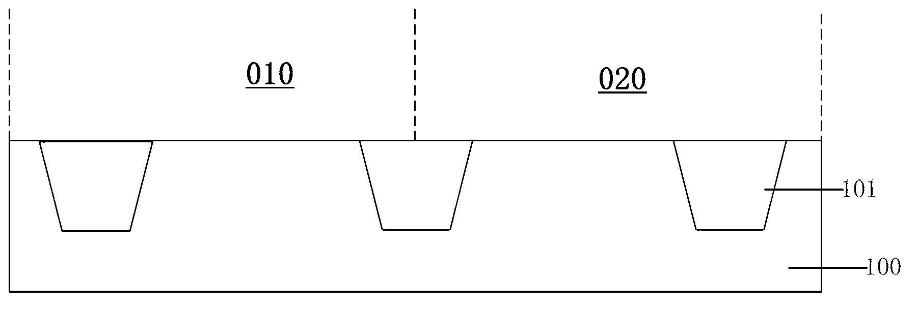
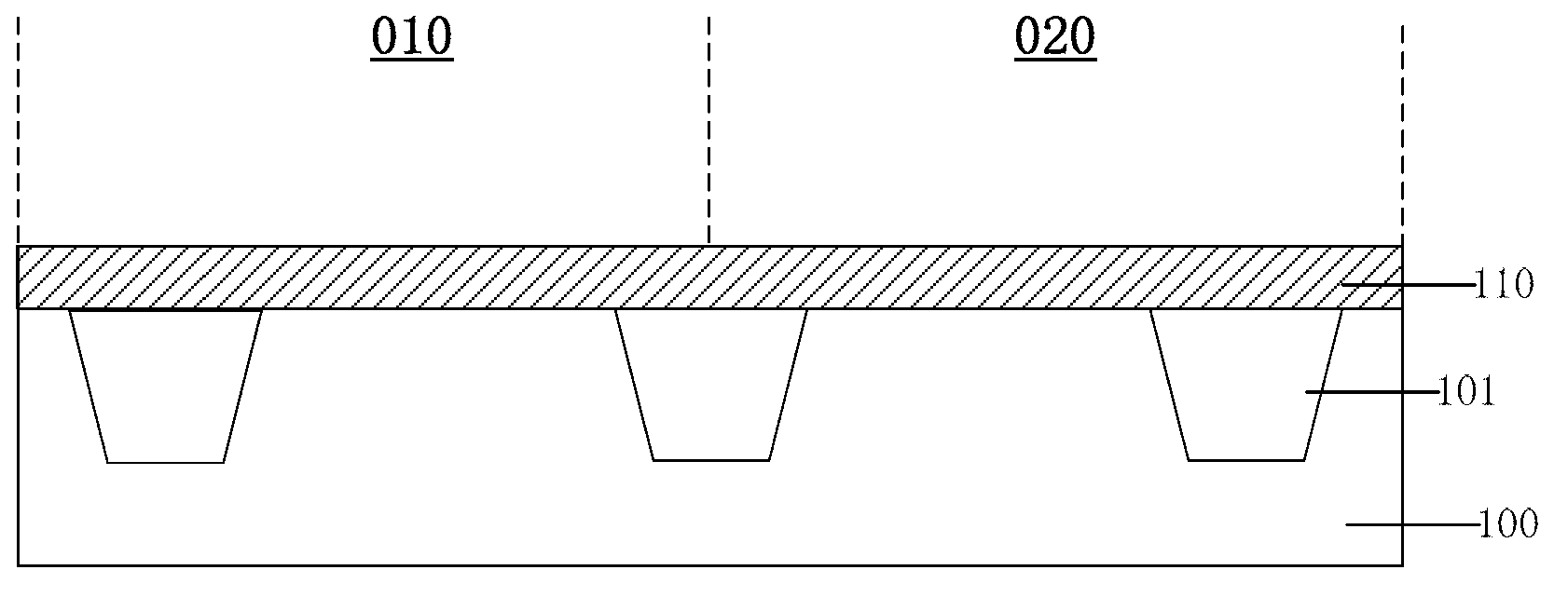
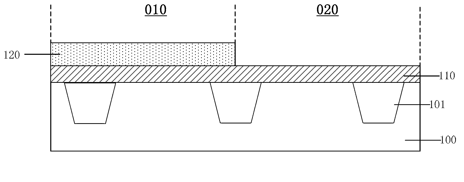
[0039] The processing method of the photoresist and the preparation method of the semiconductor device of the present invention will be described in more detail below in conjunction with the schematic diagram, wherein a preferred embodiment of the present invention is represented, and it should be understood that those skilled in the art can modify the present invention described herein, while still achieving the advantageous effects of the present invention. Therefore, the following description should be understood as the broad knowledge of those skilled in the art, but not as a limitation of the present invention.

[0040] In the interest of clarity, not all features of an actual implementation are described. In the following description, well-known functions and constructions are not described in detail since they would obscure the invention with unnecessary detail. It should be appreciated that in the development of any actual embodiment, numerous implementation details m...


PUM

PropertyMeasurementUnit
Wavelengthaaaaaaaaaa

Abstract

The invention discloses a photoresist treatment method which comprises the following steps of: providing a base on which a graphic photoresist is arranged; carrying out spin coating on a micro auxiliary film on the photoresist to form a protection film on the surface of the photoresist; treating the protection film by adopting an ultraviolet curing process. According to the photoresist treatment method, the surface density of the photoresist can be effectively increased and the defect can be avoided or reduced on the premise that the line width is guaranteed.

Description

technical field [0001] The invention relates to the technical field of semiconductor manufacturing, in particular to a photoresist processing method and a semiconductor device preparation method. Background technique [0002] Advanced integrated circuit chips usually integrate multiple functional devices. However, multiple functional devices generally need to correspond to different field effect transistors (FETs). For example, a multiple gate oxide process is a common method for fabricating different field effect transistors in the same chip. [0003] In the prior art, the multi-gate oxide structure is generally prepared by the following methods: [0004] Firstly, a substrate 100 is provided. The substrate 100 has a first region 010 and a second region 020. Generally, the substrate 100 also includes an isolation structure 101, such as Figure 1a shown; [0005] Then, prepare a silicon oxide film 110 on the substrate 100, such as Figure 1b shown; [0006] Next, prepare ...

Claims


Application Information

Patent Timeline
IPC IPC(8): G03F1/48G03F1/68H01L21/3105B05D3/06
Inventor 黄君毛智彪孟祥国
Owner SHANGHAI HUALI MICROELECTRONICS CORP
Why Eureka
Try Eureka