Method for removing low dielectric material on silicon wafer surface
A low-dielectric material and technology on the surface of silicon wafers, applied in liquid cleaning methods, chemical instruments and methods, cleaning methods and utensils, etc., can solve the problems of silicon wafer surface scrapping, reduce scrapping rate, and reduce production costs Effect
- Summary
- Abstract
- Description
- Claims
- Application Information
AI Technical Summary
Problems solved by technology
Method used
Image

Examples
Embodiment Construction
[0021] The specific embodiment of the present invention will be further described below in conjunction with accompanying drawing:
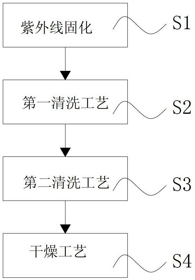
[0022] figure 1 The flow chart of the method for removing low-dielectric materials on the surface of silicon wafers specifically includes the following steps:
[0023] Step S1, providing a daily spot inspection of silicon wafers with a dielectric material deposition machine. Generally speaking, 5000A low dielectric materials are deposited on the surface of the silicon wafers, and then UV curing is performed on the silicon wafers. In the embodiment of the present invention, The reaction temperature of ultraviolet curing treatment is 350-400°C (such as 350°C, 380°C, 400°C), and the time is 280-320s (such as 280s, 290s, 300s, 320s); preferably, at a temperature of 385°C, 300s The advanced ultraviolet curing process can obtain the best technical effect, so that the low dielectric material on the surface of the silicon wafer can be cured and the subse...
PUM
 Abstract
Description
Claims
Application Information