Convex spot wire bonding method

A welding method and bump technology are applied in the field of bump wire bonding to improve the stability of bump wire bonding operations, which can solve the problems of wire bonding failure, solder ball pulling up, and detachment from bonding pads, etc., and reduce production. Cost, easy cutting, improved workability

Active Publication Date: 2013-09-11
SAMSUNG SEMICON CHINA RES & DEV +1
View PDF3 Cites 2 Cited by
  • Summary
  • Abstract
  • Description
  • Claims
  • Application Information

AI Technical Summary

Problems solved by technology

However, the hardness of copper wire is much higher than that of gold wire, so there are many problems in bump bonding, especially the tangent problem.
When cutting the wire at the top of the solder ball, especially when the wire has a high shear / tensile strength (for example, the wire is very thick, or copper wire), it is often because the wire is not easily cut and the wire is bonded. Failures, such as wire tails not forming properly, or solder balls being pulled off the pad

Method used


Image

  • Convex spot wire bonding method
  • Convex spot wire bonding method
  • Convex spot wire bonding method

Examples


Embodiment Construction

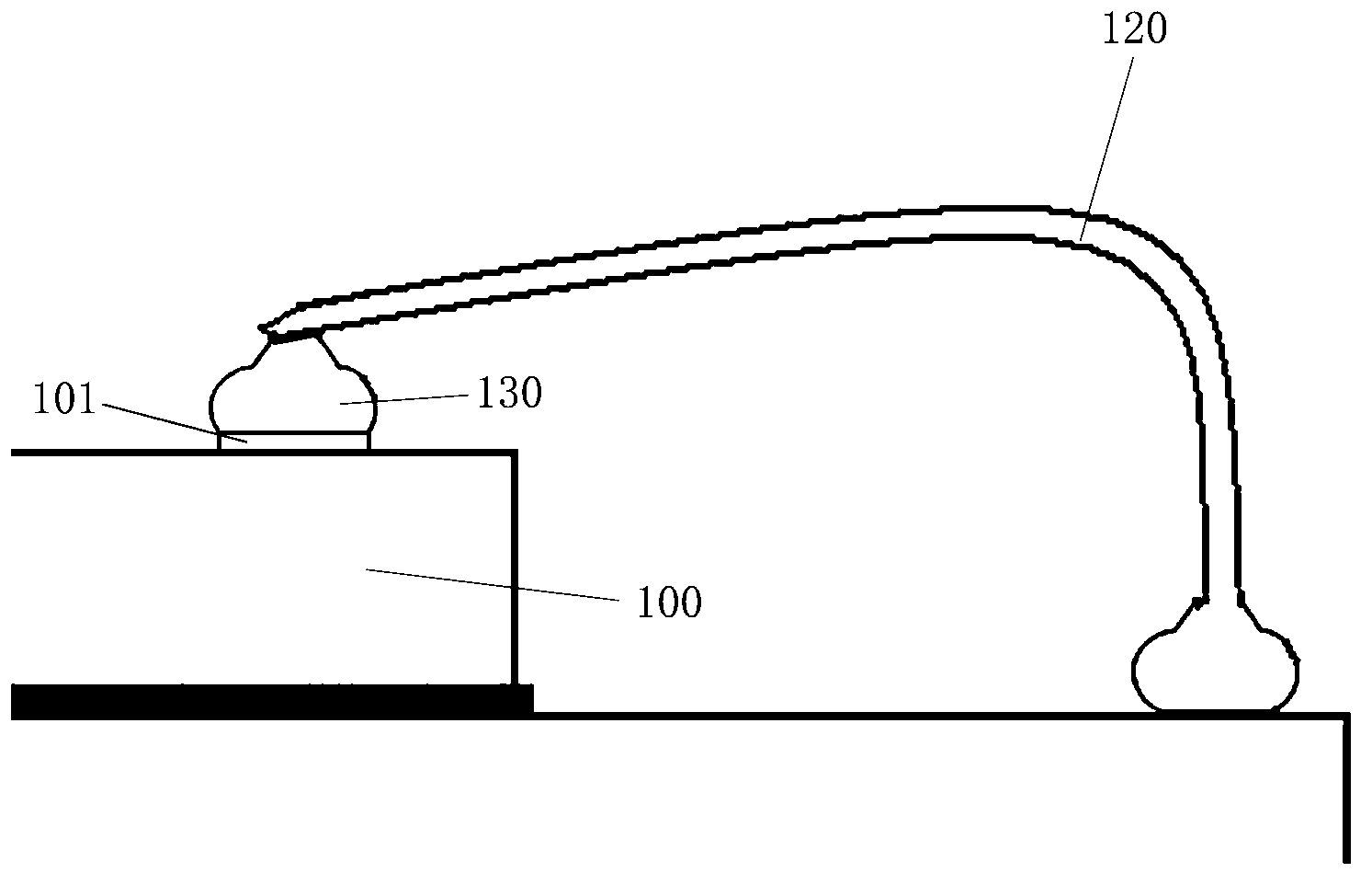
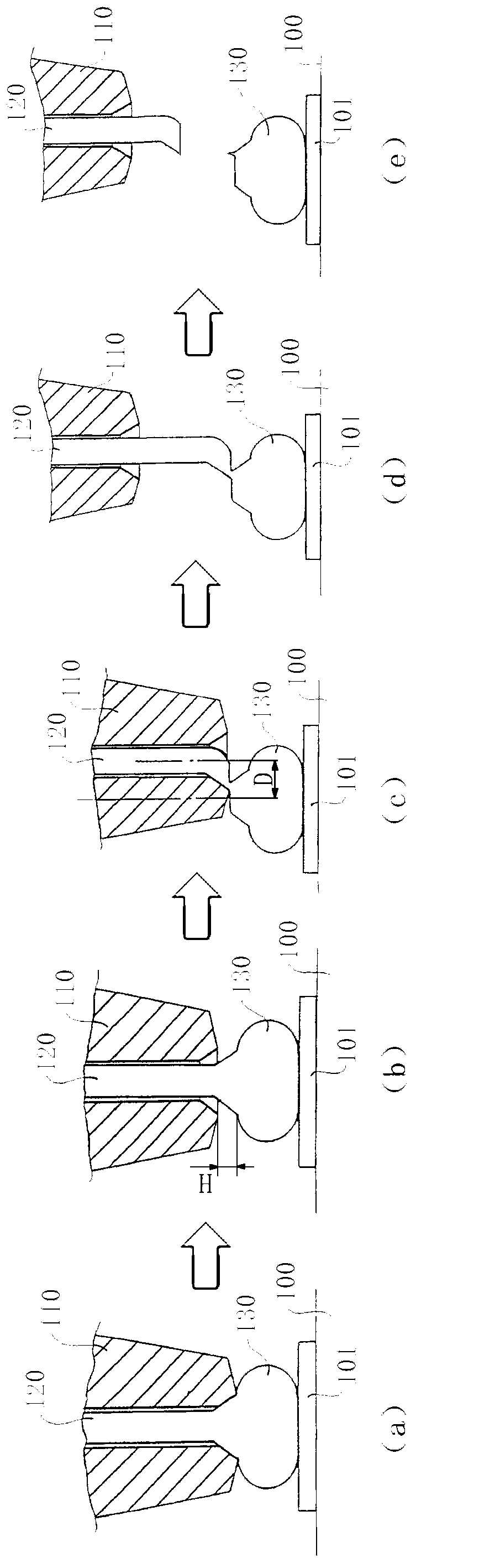
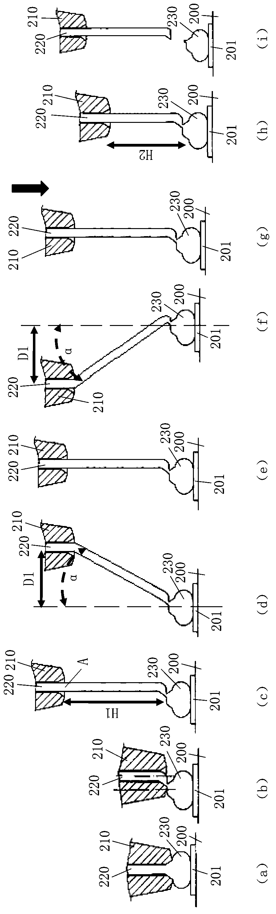
[0029] Embodiments of the invention will now be described more fully with reference to the accompanying drawings, in which exemplary embodiments of the invention are shown. However, this invention may be embodied in many different forms and should not be construed as limited to the embodiments set forth herein; rather, these embodiments are provided so that this disclosure will be thorough and complete, and will provide Those of ordinary skill in the art fully convey the concept of the embodiments of the present invention. In the following detailed description, numerous specific details are set forth by way of example in order to provide a thorough understanding of the relevant teachings. It will be apparent, however, to one skilled in the art that the present teachings may be practiced without such details. In other instances, well-known methods, procedures, components, and circuits have been described at a relatively high level and without detail in order to avoid unnecessa...


PUM


Abstract

The invention discloses a convex spot wire bonding method. The convex spot wire bonding method includes: forming weld balls via a cleaver and welding the weld balls on a weld pad; enabling connection portions of weld lines and the weld balls to deform via the cleaver so as to generate cracks; keeping the cleaver in a vertical posture, simultaneously enabling the cleaver to reciprocate along a circular arc track so as to expand crack portions of the weld lines due to a fatigue effect; and clamping the weld lines and the cleaver by a line clip, and moving upwards to snap the weld line to finish the convex spot wire bonding. According to the convex spot wire bonding method, via multiple times of reciprocation of the cleaver, the high-strength weld lines can be easily cut off by the aid of the fatigue effect, so hat production cost is reduced and operating performance is improved.

Description

technical field [0001] The invention belongs to the technical field of semiconductor packaging, in particular, the invention relates to a bump wire bonding method capable of improving the stability of the bump wire bonding operation. Background technique [0002] In order to achieve wire bonding between chips (also known as "bonding" or "bonding"), it is usually necessary to perform bump bond first. When performing bump wire bonding, it is necessary to cut the wire on the top of the solder ball after soldering the solder ball to form a bump. [0003] figure 1 A schematic diagram of bump bonding between chips in the prior art is shown. [0004] Such as figure 1 As shown, in order to electrically connect the chip 100 to a substrate (not shown), generally a chip pad (chip pad) 101 is provided on the chip, and then bumps 130 and 101 are provided on the chip pad 101 by performing a bump bonding process. Bumps (not shown) are provided on the pads (not shown) on the substrate, ...

Claims


Application Information

Patent Timeline
Patent Type & Authority Applications(China)
IPC IPC(8): H01L21/60
CPCH01L24/48H01L2224/48H01L2224/48091H01L2224/48471H01L2224/48483H01L2224/73265H01L2224/78301H01L2224/85045H01L2924/00014H01L2924/00012H01L2224/4554
Inventor 周永华
Owner SAMSUNG SEMICON CHINA RES & DEV
Why Eureka
Try Eureka