Method for forming fin transistors

A fin transistor and fin technology, which is applied in semiconductor devices, semiconductor/solid-state device manufacturing, electrical components, etc., can solve the problems of low yield and poor electrical performance uniformity of fin transistors, and achieves good thickness uniformity and thickness. Controllable effect

Active Publication Date: 2015-12-16
SEMICON MFG INT (SHANGHAI) CORP +1
View PDF7 Cites 0 Cited by
  • Summary
  • Abstract
  • Description
  • Claims
  • Application Information

AI Technical Summary

Problems solved by technology

[0004] However, the uniformity of electrical properties of fin transistors formed by the prior art is poor, and the yield rate is low

Method used


Image

  • Method for forming fin transistors
  • Method for forming fin transistors
  • Method for forming fin transistors

Examples


Embodiment Construction

[0014] It can be seen from the background technology that the fin transistors formed in the prior art have poor electrical performance uniformity and low yield rate. Therefore, the inventors of the present invention researched the fin transistor formation methods in the prior art and found that the fin transistors in the prior art The method for forming a transistor includes the following steps:

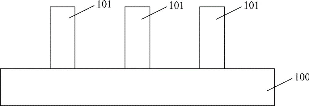
[0015] Please refer to figure 2 , providing a substrate 100, the surface of the substrate 100 is formed with a plurality of fins 101;

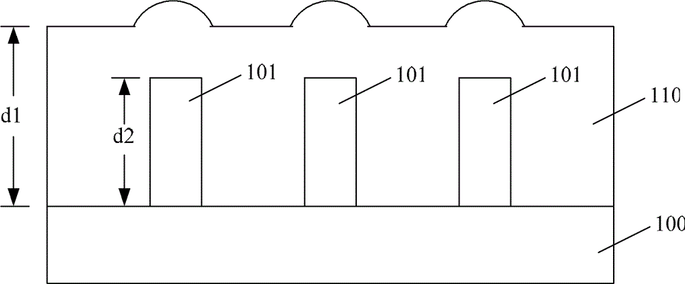
[0016] Please refer to image 3 , forming a polysilicon layer 110 across the fin portion 101 on the surface of the substrate 100; the polysilicon layer 110 is used as a dummy gate of the fin transistor, the polysilicon layer 110 covers part of the sidewall of the fin portion 101, and the polysilicon layer The thickness (d1) of 110 is greater than the thickness (d2) of the fin portion 101;

[0017] The formation process of the polysilicon layer 11...


PUM


Abstract

The invention provides a forming method of a fin type transistor. The method comprises the following steps that a substrate is provided, a plurality of fin parts are formed on the surface of the substrate, a blocking layer is arranged on the top surface of the fin parts, a first covering layer covering the fin parts is formed on the surface of the substrate, the first covering layer is flattened until the blocking layer is exposed, a second covering layer is formed on the surfaces of the blocking layer and the first covering layer by adopting a deposition process; and the second covering layer and the first covering layer are etched, and pseudo grids are formed. The forming method of the fin type transistor provided by the embodiment has the advantage that the qualification rate is high.

Description

technical field [0001] The invention relates to the field of semiconductor manufacturing, in particular to a method for forming a fin transistor. Background technique [0002] With the continuous development of semiconductor process technology, process nodes are gradually reduced, and gate-last (gate-last) process has been widely used to obtain an ideal threshold voltage and improve device performance. However, when the feature size (CD, Critical Dimension) of the device is further reduced, even if the gate-last process is adopted, the structure of the conventional MOS field effect transistor can no longer meet the requirements for device performance, and multi-gate devices have been widely used as a substitute for conventional devices. s concern. [0003] Fin transistor (FinFET) is a common multi-gate device, figure 1 A schematic diagram of a three-dimensional structure of a fin transistor in the prior art is shown. Such as figure 1 As shown, the fin transistor includes...

Claims


Application Information

Patent Timeline
Patent Type & Authority Patents(China)
IPC IPC(8): H01L21/28H01L21/336
Inventor 洪中山
Owner SEMICON MFG INT (SHANGHAI) CORP
Why Eureka
Try Eureka