Blind-buried hole interconnecting structure and processing method therefor

A technology of conduction structure and blind buried via, which is applied in the direction of electrical connection of printed components, formation of electrical connection of printed components, printed circuit components, etc., can solve the problems of poor conduction/isolation, high processing cost, and high metallization process requirements. , to solve the high risk of reliability testing, reduce alignment requirements, and ensure product quality.

Inactive Publication Date: 2016-06-01
JIANGSU PROVISION ELECTRONICS CO LTD
View PDF8 Cites 0 Cited by
  • Summary
  • Abstract
  • Description
  • Claims
  • Application Information

AI Technical Summary

Problems solved by technology

[0003] First of all, it is necessary to realize the conduction of components between multi-layer circuit boards, and at the same time, it corresponds to the high alignment requirements of all layers of the circuit board. Any layer alignment deviation will lead to poor conduction / isolation, and the production is difficult;
[0004] Secondly, when the circuit board is a deep through hole (aspect ratio > 10:1), the metallization process of the entire hole wall is required to be high. When the metallization thickness in the center of the deep through hole is likely to be insufficient, it will cause poor contact or even breakage in the reliability test. Risk, more seriously, the center of the deep via hole cannot be metallized, which directly leads to poor conductivity;
[0005] Secondly, the production efficiency is low. When the diameter of the drill remains unchanged, the number of drilled stacks will decrease with the increase of the thickness of the circuit board;
[0006] Finally, the cost of drilling needles is high. When the processing aperture is ≤0.15mm, the cost of mechanical drilling is more than 5 times higher than that of laser drilling, and the smaller the aperture, the more significant the difference

Method used


Image

  • Blind-buried hole interconnecting structure and processing method therefor
  • Blind-buried hole interconnecting structure and processing method therefor
  • Blind-buried hole interconnecting structure and processing method therefor

Examples


Embodiment Construction

[0037] A preferred embodiment of the present invention will be described in detail below in conjunction with the accompanying drawings. However, the scope of protection of the present invention is not limited to the following examples, that is, any simple equivalent changes and modifications made based on the patent scope of the present invention and the content of the description are still within the scope of the patent of the present invention.

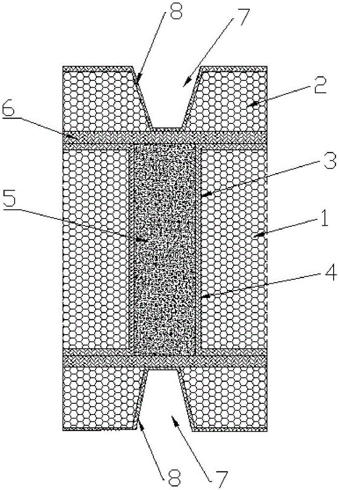
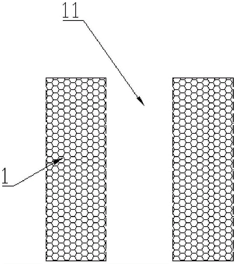
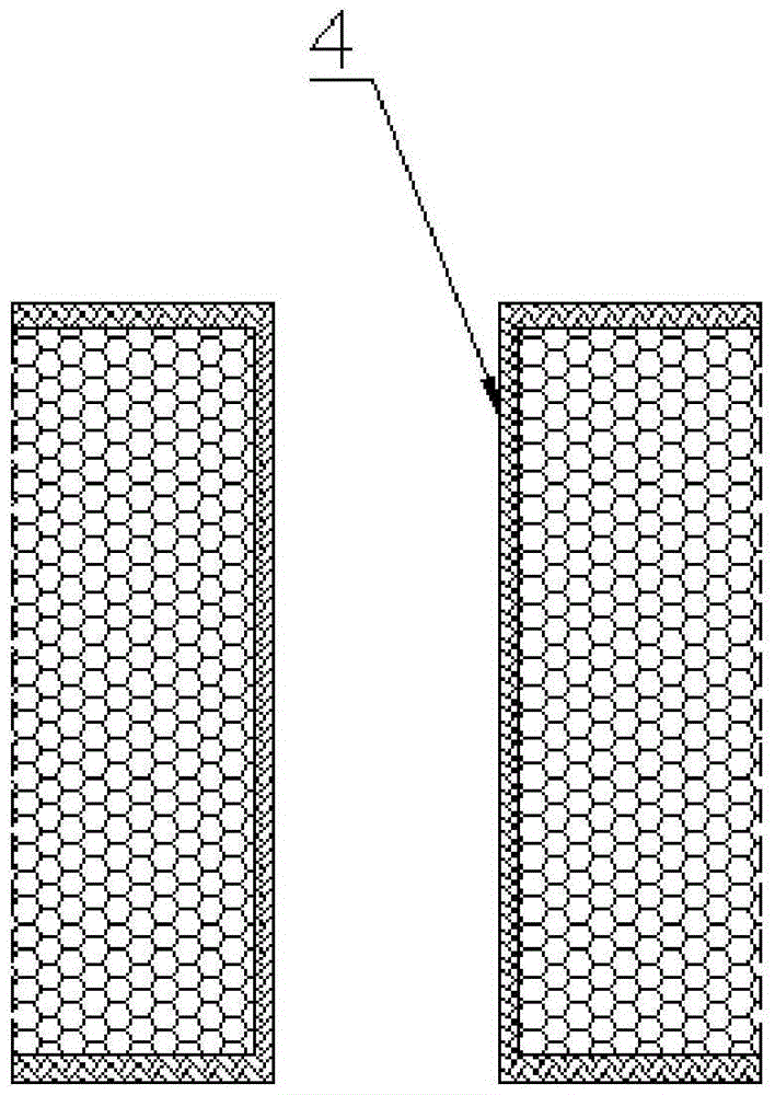
[0038] Such as figure 1 As shown, a blind buried hole interconnection conduction structure includes an inner core board 1 and two side boards 2 located on both sides of the inner core board, and the inner core board is formed by mechanical drilling to form a central buried Hole 3, the hole wall of the central buried hole is metallized to form a metal conduction layer 4 in the central hole, the hole of the central buried hole is filled with non-conductive material 5 epoxy resin, the two hole ports of the central buried hole And the ...


PUM


Abstract

The invention discloses a blind-buried hole interconnecting structure and a processing method therefor. Laser blind hole and mechanical buried hole interconnection is adopted to replace the conventional mechanical through hole, so that the alignment requirement of layers of a circuit board part is lowered, and the manufacturing difficulty is lowered; a high aspect ratio of a deep through hole is converted to a low aspect ratio of a mechanical buried hole; the buried hole in an inner layer core plate and the blind hole in a side plate are subjected to metallization processing in different steps; the metallization process is simple, and the thickness controllability is high, so that the technical problem that the center of a deep hole cannot be metalized is solved; the technical problem of high reliability test risk caused by insufficient metallization thickness of the deep through hole is solved consequently; the yield is improved and the product quality is ensured; the technical problem that the flexible design specific to a circuit board cannot be realized caused by limitation of the conventional mechanical through hole is solved; therefore, the production cost is lowered and the production efficiency is improved; the processing method is suitable for processing various circuit boards greater than or equal to 3L needing to be conducted through the mechanical through holes; and the processing method particularly has obvious advantages in processing of deep through hole circuit boards with the aspect ratio of greater than 10:1.

Description

technical field [0001] The invention relates to the technical field of PCB processing, in particular to a blind buried hole interconnection structure and a processing method thereof. Background technique [0002] At present, in the field of PCB processing technology, mechanical through holes are used to carry hole wall metallization to achieve interlayer conduction, but there are many problems: [0003] First of all, it is necessary to realize the conduction of components between multi-layer circuit boards, and at the same time, it corresponds to the high alignment requirements of all layers of the circuit board. Any layer alignment deviation will lead to poor conduction / isolation, and the production is difficult; [0004] Secondly, when the circuit board is a deep through hole (aspect ratio > 10:1), the metallization process of the entire hole wall is required to be high. When the metallization thickness in the center of the deep through hole is likely to be insufficient...

Claims


Application Information

Patent Timeline
Patent Type & Authority Applications(China)
IPC IPC(8): H05K1/11H05K3/42
CPCH05K1/115H05K3/421H05K2201/09509H05K2201/09536
Inventor 马洪伟唐高生
Owner JIANGSU PROVISION ELECTRONICS CO LTD
Why Eureka
Try Eureka