
Eureka
For R&D, Eureka makes reading and utilizing patents & technical documents easy.
Eureka AIR
Designed for self-driven R&D workflows. Generate viable solutions, solve complex R&D challenges, empower your innovation with AI.

Eureka Materials
Designed for material experts only. Revolutionize your material R&D, from search, analyze, to developing new materials.

TechResearch
Generate reliable direction feasibility study reports for your R&D in just a few steps.

TechSeek
Discover and master advanced knowledge NOW. Basics, ideas, possibilities, all at once.

TechMind
As an expert in R&D Theories, TechMind can generates customized viable solutions instantly.

TechRisk
Analyze your overall solution with one click, know your potential R&D risks in advance.

TechMonitor
Get weekly tech updates, stay abreast of the latest tech innovations and key insights.
Formation method of transistor
A technology of transistors and semiconductors, applied in the fields of semiconductor/solid-state device manufacturing, electrical components, circuits, etc., can solve the problems of limited improvement in transistor performance, limited stress, and small increase in carrier mobility, so as to improve mobility, improve effect of stress
- Summary
- Abstract
- Description
- Claims
- Application Information
AI Technical Summary
Problems solved by technology
Method used
Image


Examples
Embodiment Construction
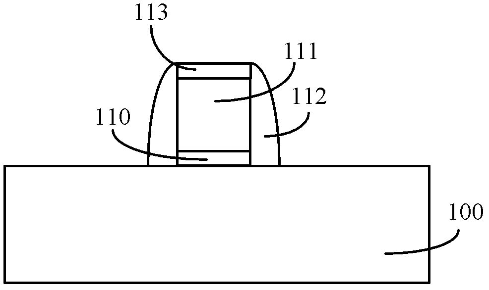
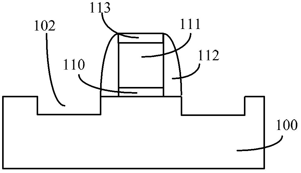
[0042] As mentioned in the background technology, in the transistor with stress liner layer formed in the prior art, the stress increase of the source / drain region is limited, and the improvement of the carrier mobility of the channel region is small, resulting in the performance of the formed transistor Improvement is limited.
[0043] After research, the inventor found that the reason for the small increase in the mobility of carriers in the channel region is the distance from the apex of the stress liner layer to the extension line of the boundary of the gate electrode layer, and the distance from the apex of the stress liner layer to the semiconductor substrate The distance from the surface is related; the closer the distance from the top corner of the stress liner layer to the extension line of the boundary of the gate electrode layer is, the greater the stress generated in the channel region is, and the higher the mobility of carriers in the channel of the formed transist...
PUM
 Abstract
Description
Claims
Application Information
 - R&D Engineer
- R&D Manager
- IP Professional
- Industry Leading Data Capabilities
- Powerful AI technology
- Patent DNA Extraction
Browse by: Latest US Patents, China's latest patents, Technical Efficacy Thesaurus, Application Domain, Technology Topic, Popular Technical Reports.
© 2024 PatSnap. All rights reserved.Legal|Privacy policy|Modern Slavery Act Transparency Statement|Sitemap|About US| Contact US: help@patsnap.com