Encapsulating piece for preventing chip salient point from being short-circuited and manufacturing process thereof

A packaging and manufacturing process technology, applied in semiconductor/solid-state device manufacturing, circuits, electrical components, etc., can solve problems such as voids in plastic packaging materials, reduction of chips and frames, and impact on product reliability.

Inactive Publication Date: 2013-09-18
HUATIAN TECH XIAN
View PDF4 Cites 14 Cited by
  • Summary
  • Abstract
  • Description
  • Claims
  • Application Information

AI Technical Summary

Problems solved by technology

However, due to the limitations of traditional packaging in the past, the chip bumps melted and collapsed during the reflow process, causing a short circuit between the two chip bump

Method used


Image

  • Encapsulating piece for preventing chip salient point from being short-circuited and manufacturing process thereof
  • Encapsulating piece for preventing chip salient point from being short-circuited and manufacturing process thereof
  • Encapsulating piece for preventing chip salient point from being short-circuited and manufacturing process thereof

Examples


specific Embodiment approach

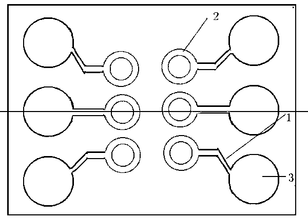
[0028] The specific implementation method is: the copper plate is processed into figure 1 As shown in the frame design, then, the chip bump 5 is dipped in flux, and the chip bump 5 is combined with the copper surface in the corresponding ring-shaped copper pillar 2 through a flip-chip loading machine, and an effective soldering junction is formed under the action of reflow soldering. , the chip bump diameter is 0.2mm, the chip bump height is 0.13mm, and the material is Sn96.5%Ag3.0%Cu0.5%. Finally, the residual flux on the chip bumps 5 is cleaned with plasma water having a resistivity of 1.0 m / Ω.mm or more. The reflux temperature is 260°C, the reflux time is 50~70s, the cleaning temperature is 42°C, the pressure is 40psi, and the cleaning transmission speed is 0.8m / min.

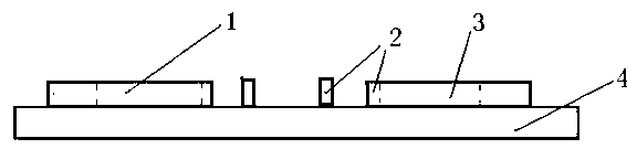
[0029] The function of several materials used: the function of the ring-shaped copper pillar 2 is to prevent the chip bump 5 from collapsing due to melting during the reflow process, causing the chip bump 5...


PUM


Abstract

The invention discloses an encapsulating piece for preventing a chip salient point from being short-circuited and a manufacturing process thereof. The encapsulating piece mainly comprises a copper circuit, an annular copper column, a copper column, a copper plate, a chip salient point, a chip, a molten chip salient point, a plastic package body, a copper column left after back side etching, a green oil layer and a tin ball, wherein the copper circuit, the annular copper column and the copper column are arranged on the copper plate; the molten chip salient point is bonded in the annular copper column; the chip is arranged at the chip salient point; the left copper column is formed after back side etching of the copper plate; the green oil layer is formed on the back side of the copper plate; the tin ball is arranged on the copper column left after back side etching; the plastic package body surrounds the upper surface of the copper plate, the copper circuit, the annular copper column, the copper column and the chip to form an integral circuit; and the chip, the chip salient point on the chip, the annular copper column and the copper column left after back side etching construct a power supply and a signal channel. The process flow comprises wafer thinning, wafer scribing, reserve chip loading, reflow cleaning, plastic package, etching for separating pins, filling green paint, printing and reballing of a steel screen, printing, cutting, packing and delivering. Due to the adoption of the encapsulating piece, short circuit between two chip salient points can be prevented, and the reliability of a product is improved.

Description

technical field [0001] The invention relates to the technical field of manufacturing electronic information automation components, in particular to a package for preventing chip bumps from short-circuiting and a manufacturing process thereof. Background technique [0002] Flip Chip is not only a chip interconnection technology, but also an ideal chip bonding technology. As early as 30 years ago, IBM has developed and used this technology. But until recent years, Flip-Chip has become a frequently used packaging form in the field of high-end devices and high-density packaging. Today, the application range of Flip-Chip packaging technology is becoming wider and wider, and the packaging forms are becoming more diversified, so the requirements for Flip-Chip packaging technology are also increasing. At the same time, Flip-Chip also poses a series of new serious challenges to manufacturers, providing reliable support for packaging, assembly and testing for this complex technology...

Claims


Application Information

Patent Timeline
IPC IPC(8): H01L23/488H01L21/50
CPCH01L2224/11
Inventor 王虎朱文辉谌世广钟环清刘卫东
Owner HUATIAN TECH XIAN
Why Eureka
Try Eureka