FCQFN encapsulation part preventing solder balls from collapsing and manufacturing process of FCQFN encapsulation part

A manufacturing process and packaging technology, used in semiconductor/solid-state device manufacturing, electrical components, electrical solid-state devices, etc., can solve problems such as chip and frame reduction, plastic packaging voids, and impact on product reliability.

Active Publication Date: 2013-09-25
HUATIAN TECH XIAN
View PDF4 Cites 6 Cited by
  • Summary
  • Abstract
  • Description
  • Claims
  • Application Information

AI Technical Summary

Problems solved by technology

However, due to the limitations of traditional packaging in the past, the chip bumps melted and collapsed during the reflow process, causing a short circuit between the two chip b...

Method used


Image

  • FCQFN encapsulation part preventing solder balls from collapsing and manufacturing process of FCQFN encapsulation part
  • FCQFN encapsulation part preventing solder balls from collapsing and manufacturing process of FCQFN encapsulation part
  • FCQFN encapsulation part preventing solder balls from collapsing and manufacturing process of FCQFN encapsulation part

Examples


Embodiment approach

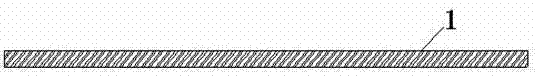
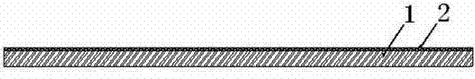
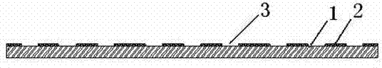
[0029] The specific implementation method is: the first layer of green paint 2 (photosensitive resist material) is coated on a specific area of ​​the copper lead frame 1 by screen printing, exposed and developed after drying, and formed as image 3 The green paint groove 3 shown has a groove depth of about 30 μm, an opening of about 0.22 mm, and a copper lead frame thickness defined as 0.127 mm. Then, the tin-silver-copper bump 5 is dipped in flux, and the tin-silver-copper bump 5 is combined with the copper surface in the corresponding green paint groove 3 through a flip-chip machine, and an effective solder joint is formed under the action of reflow soldering, and the chip The diameter of the bump is 0.2mm, the height of the tin-silver-copper bump 5 is 0.13mm, and the material is Sn96.5%Ag3.0%Cu0.5%. Finally, the residual flux on the tin-silver-copper bumps 5 is cleaned with plasma water having a resistivity of 1.0 m / Ω.mm or more. The reflux temperature is 260°C, the reflux...


PUM


Abstract

The invention discloses an FCQFN encapsulation part preventing solder balls from collapsing and a manufacturing process of the FCQFN encapsulation part. The encapsulation part is mainly composed of a copper lead frame, a first green paint layer, green paint grooves, chips, tin-silver-copper protruded points, a plastic packaging body, etched pins, a second green paint layer and the solder balls. The first green paint layer coats the copper lead frame and is provided with the green paint grooves, and the chips and the tin-silver-copper protruded points are adhered to the green paint grooves. The plastic packaging body wraps the upper surface of the copper lead frame, the first green paint layer, the green paint grooves, the chips and the tin-silver-copper protruded points to form an overall circuit. The etched pins are formed by the etched copper lead frame, the etched copper lead frame comprises an etching thinning area, the second green paint layer coats the inside of the etching thinning area, and the solder balls are located on the etched pins. The manufacturing process comprises the following steps of wafer thinning, wafer scribing, green paint coating of the frame, exposure development, inverse chip assembly, backflow cleaning, plastic packaging, thinning of the back face of the frame, etching and separation of the pins, green paint filling, steel mesh printing and ball mounting, cutting, packaging and delivery. According to the FCQFN encapsulation part preventing the solder balls from collapsing and the manufacturing process of the FCQFN encapsulation part, short circuit is prevented, filling performance of plastic packaging materials is improved, and therefore product reliability is promoted.

Description

technical field [0001] The invention relates to the technical field of manufacturing electronic information automation components, in particular to an FCQFN package for preventing tin ball collapse and a manufacturing process thereof. Background technique [0002] Flip Chip is not only a chip interconnection technology, but also an ideal chip bonding technology. As early as 30 years ago, IBM has developed and used this technology. But until recent years, Flip-Chip has become a frequently used packaging form in the field of high-end devices and high-density packaging. Today, the application range of Flip-Chip packaging technology is becoming wider and wider, and the packaging forms are becoming more diversified, so the requirements for Flip-Chip packaging technology are also increasing. At the same time, Flip-Chip also poses a series of new serious challenges to manufacturers, providing reliable support for packaging, assembly and testing for this complex technology. In th...

Claims


Application Information

Patent Timeline
IPC IPC(8): H01L23/495H01L21/60
CPCH01L24/97H01L2224/16H01L2924/15747H01L2924/00
Inventor 谌世广朱文辉刘卫东钟环清谢天禹
Owner HUATIAN TECH XIAN
Why Eureka
Try Eureka