Image pickup device and method for manufacturing same

A technology of a camera device and a manufacturing method, which are applied in the directions of installation, image communication, instruments, etc., can solve problems such as difficulty in processing the camera device, and achieve the effects of shortening positioning operations and improving manufacturing efficiency.

Inactive Publication Date: 2013-09-18
OLYMPUS CORP
View PDF4 Cites 1 Cited by
  • Summary
  • Abstract
  • Description
  • Claims
  • Application Information

AI Technical Summary

Problems solved by technology

[0004] However, in the case of an imaging device having a prism that allows light to enter from a direction intersecting the optical axis of the imaging element like a prism that is bonded like a triangular prism, and uses a reflective surface to reflect the incident light to enter the imaging element. , since the reflective surface is arranged obliquely with respect to the imaging element, it is difficult to process it by the imaging device formed into a single piece after adsorption and cutting

Method used


Image

  • Image pickup device and method for manufacturing same
  • Image pickup device and method for manufacturing same
  • Image pickup device and method for manufacturing same

Examples


Embodiment Construction

[0050] Hereinafter, an imaging device 1 and a manufacturing method thereof according to an embodiment of the present invention will be described with reference to the drawings.

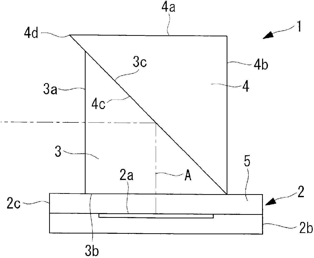
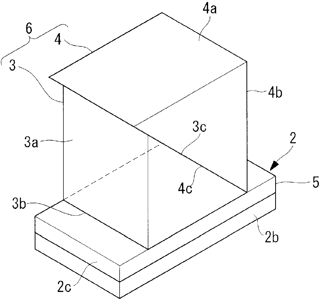
[0051] Such as figure 1 with figure 2 As shown, the imaging device 1 of this embodiment includes a flat imaging element 2 , a triangular prism 3 fixed to the surface of the imaging element 2 , and a cover member 4 fixed to cover the triangular prism 3 . In the drawings, reference numeral 5 is a transparent cover glass covering the imaging surface 2 a of the imaging element 2 and constituting a part of the imaging element 2 .

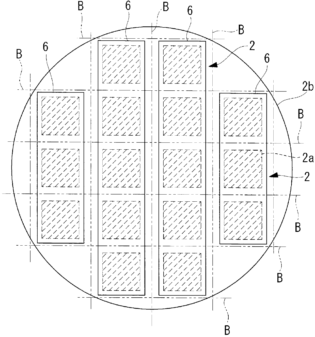
[0052] The imaging element 2 is manufactured on a silicon wafer by semiconductor manufacturing technology, has an imaging surface 2a on which light is incident, and forms an image by converting light incident on the imaging surface 2a into an electrical signal.

[0053] The triangular prism 3 comprises a mutually orthogonal incident surface 3a and an outgoing surface 3b, and ...


PUM


Abstract

This image pickup device can be easily manufactured, and can be handled by being easily sucked even in an individually separated state. Provided is an image pickup device (1) having: an image pickup element (2); a prism (3), which is fixed to the image pickup element (2), and has a light input surface (3a) having light inputted thereto from the direction intersecting an optical axis (A) of the image pickup element (2), a light output surface (3b) substantially parallel to the image pickup surface (2a) of the image pickup element (2), and a reflecting surface (3c) that deflects the light inputted to the light input surface (3a) to the direction along the optical axis (A) of the image pickup element (2); and a cover member (4), which is fixed at a position that covers the reflecting surface (3c) of the prism (3), and has an outer surface (4a) substantially parallel to the image pickup surface (2a).

Description

technical field [0001] The invention relates to an imaging device and a manufacturing method thereof. Background technique [0002] Conventionally, a method of manufacturing a plurality of optical heads by bonding rod-shaped prisms to a plurality of semiconductor elements produced on a silicon wafer and then cutting the integrally formed silicon wafer, semiconductor elements, and prisms is known. [0003] Patent document: Japanese Patent Laid-Open No. 63-127444 [0004] However, in the case of an imaging device having a prism that allows light to enter from a direction intersecting the optical axis of the imaging element like a prism that is bonded like a triangular prism, and uses a reflective surface to reflect the incident light to enter the imaging element. , since the reflective surface is arranged obliquely with respect to the imaging element, it is difficult to handle it by the imaging device formed into a single piece after suction cutting. Contents of the inventi...

Claims


Application Information

Patent Timeline
Patent Type & Authority Applications(China)
IPC IPC(8): H04N5/225G02B7/18
CPCH01L27/14618H01L27/14623H01L27/14625H01L2924/0002H04N23/57H04N23/55H01L2924/00
Inventor 折原达也金野光次郎
Owner OLYMPUS CORP
Why Eureka
Try Eureka