Bearing device and method adopting same to transfer wafers

A technology of a carrier device and a wafer, applied in the field of carrier device and wafer transfer, can solve the problems of lamination danger, reduced utilization rate of process equipment, and no disclosure of technical features of wafers with special morphology.

Active Publication Date: 2013-09-25
SHANGHAI HUALI MICROELECTRONICS CORP
View PDF7 Cites 3 Cited by
  • Summary
  • Abstract
  • Description
  • Claims
  • Application Information

AI Technical Summary

Problems solved by technology

[0006] However, when the edge of the wafer placed on the carrier platform has a special shape, such as image 3 As shown, when placing a wafer 16 with a special shape (such as a notch 15 on the edge of the wafer), and if the nozzle 14 is in contact with the wafer 16 with a special shape at the notch 15, a gap will be formed, and the nozzle 14 The sprayed deionized water leaks from the gap, thereby reducing the resistance of the wafer 16 with a special shape to the deionized water sprayed by the nozzle 14, so that the converter outputs a higher voltage after conversion, that is, when there is a gap 15 ( When the wafer 16 with a step structure formed on the edge of the wafer 13 is placed on the carrying platform, the ionized water leaks from the gap formed, so that the converter outputs a higher voltage, and the corresponding wafer sensor 12 cannot detect the wafer with a special shape. The existence of the wafer 16 of the appearance, and then will cause the danger of lamination
In addition, since the wafer sensor 12 is fixed, it can only detect and identify wafers of one size and specification. When performing CMP process on wafers of different specifications, it is necessary to replace the sensors of corresponding specifications, thereby reducing the cost of process equipment. Mobility
[0007] Chinese patent (authorized announcement number: CN101511539B) describes a planarized grinding device and grinding method. By setting multiple reference signals in multiple areas on the substrate, a uniform film thickness can be obtained on the entire area of ​​the substrate, and There is no need to make the sensor close to the ground surface of the substrate in order to narrow the effective measurement range of the sensor, so that there are no through-holes or backside pits and other grinding deposits (pad); Technical features, it is unavoidable that the sensor cannot detect the wafer due to defects such as a stepped structure, and then form a laminate, and the process can only be performed on a wafer of one specification
[0008] Chinese patent (application publication number: CN102802871A) discloses a grinding device, a grinding pad and a grinding information management system. By embedding sensors, memory, drivers and communicators in the grinding pad, the information is managed in a unified way, so that it can be easily Perform operations such as adjusting the operating conditions and analyzing the occurrence of poor grinding; the technical solution does not disclose the relevant technical features of detecting wafers with special shapes, which cannot be avoided due to defects such as step structures, which cause the sensor to fail to detect Wafers, and then the emergence of laminations, and can only be processed for one specification of wafers

Method used


Image

  • Bearing device and method adopting same to transfer wafers
  • Bearing device and method adopting same to transfer wafers
  • Bearing device and method adopting same to transfer wafers

Examples


Embodiment Construction

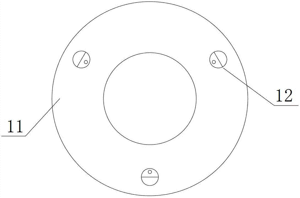
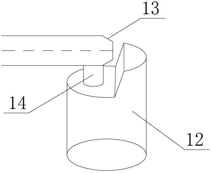
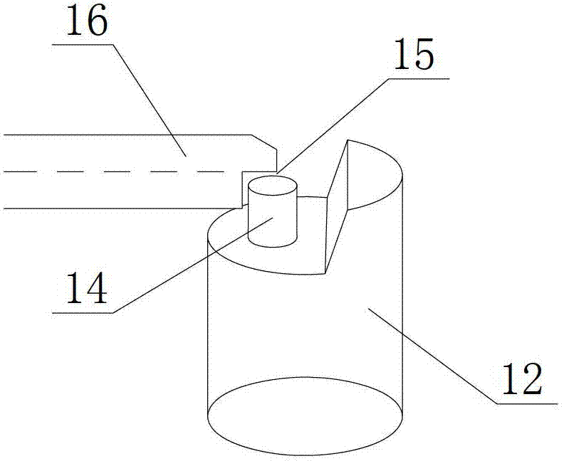
[0032] Figure 4 It is a structural schematic diagram of the grinding device of the present invention; as Figure 4 As shown, a carrier device of the present invention has a technical node of 90nm, 65 / 55nm, 45 / 40nm or 32 / 28nm, etc., and is mainly used in the chemical mechanical polishing process of wafers. The carrier device includes a circular carrier platform 21 , the carrying platform 21 can be an input platform (input station) or an output platform (output station) for carrying wafers in a grinder table (such as CMP, etc.), and the carrying platform 21 is provided with evenly distributed guide rails 22, preferably Set up 3 rails like Figure 4 As shown, the three guide rails 22 are evenly distributed on the carrying platform 21 at an angle of 120° to each other to fix the wafer, and each guide rail 22 is provided with a sensor 23, and the sensor 23 is placed on the carrying platform 21 along the guide rail 22. can move back and forth in the radial direction.

[0033] Wh...


PUM


Abstract

The invention generally relates to the field of manufacture of semiconductor integrated circuits, particularly to a bearing device and a method adopting the device to transfer wafers. In the bearing device and the method adopting the device to transfer wafers, a movable sensor is arranged on a bearing platform, the position of the sensor can be set as per wafers of different specifications and sizes, so that the movable sensor can be used for recognizing and detecting wafers of different sizes and accurately detecting and recognizing wafers with special shapes, and overlapped wafers in a bearing platform can be effectively avoided, the danger of crushing wafers as wafers cannot be recognized is reduced, the yield of products is improved, the process cost is reduced, little modification is carried out to the conventional equipment, and the compatibility of the device is stronger.

Description

technical field [0001] The present invention generally relates to the field of semiconductor integrated circuit manufacturing, more precisely, the present invention relates to a carrying device and a wafer transfer method using the device. Background technique [0002] At present, with the continuous advancement of semiconductor integrated manufacturing technology, its performance has been continuously improved, and with the integration process of device miniaturization and miniaturization, the planarization process of semiconductor wafers has become a very critical technology in the field of semiconductor manufacturing. In particular, chemical mechanical polishing (CMP) technology has been widely used. [0003] In the CMP grinding process, the input port (PIN), output port (POUT) and HCLU of the carrying platform are equipped with wafer sensors (wafer sensors) for identifying wafers (wafers), and only identified wafers can enter the grinding process The device performs the...

Claims


Application Information

Patent Timeline
Patent Type & Authority Applications(China)
IPC IPC(8): B24B37/27H01L21/683
Inventor 张冬芳张守龙白英英陈玉文蒋德念
Owner SHANGHAI HUALI MICROELECTRONICS CORP
Why Eureka
Try Eureka