Filter circuit of integrated circuit and integrated circuit

A filter circuit and integrated circuit technology, which is applied in the direction of fail-safe circuits, electrical components, and electric pulse generation, can solve problems such as input signal interference, high-voltage integrated circuits and application system damage, and achieve the effect of reducing the probability of damage

Active Publication Date: 2013-09-25
上海奔赛电子科技发展有限公司
View PDF3 Cites 10 Cited by
  • Summary
  • Abstract
  • Description
  • Claims
  • Application Information

AI Technical Summary

Problems solved by technology

[0009] The invention aims at the problem that the input signal of the integrated circuit will be disturbed by the outside, which will cause the MOS tube or IGBT driven by the integrated circuit to break

Method used


Image

  • Filter circuit of integrated circuit and integrated circuit
  • Filter circuit of integrated circuit and integrated circuit
  • Filter circuit of integrated circuit and integrated circuit

Examples


Embodiment 1

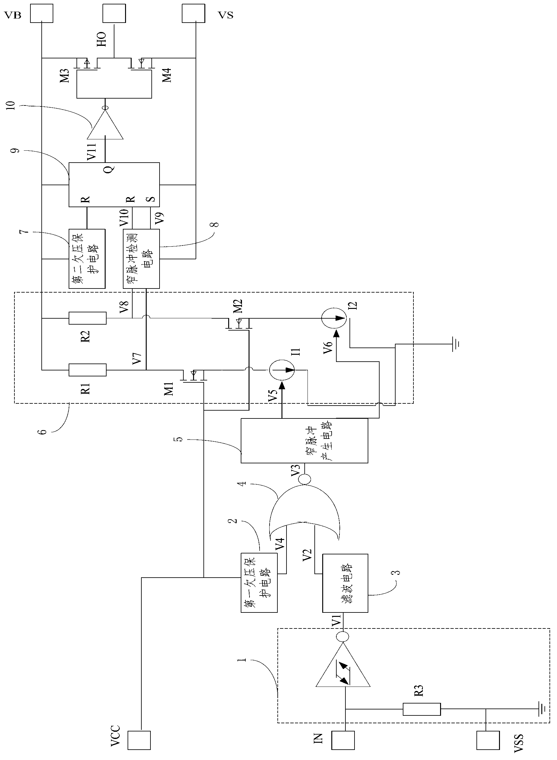
[0050] Such as Figure 7 As shown, the filter circuit of the integrated circuit provided by this embodiment includes a low-level delay unit 21, whose input terminal receives the input signal VIN, and is used to delay the falling edge of the received input signal and output it; the first filter unit 22, connected with the low-level delay unit 21, used to filter out the negative pulse whose pulse width is less than the delay time of the low-level delay unit 21; the high-level delay unit 31, whose input terminal receives the input The signal VIN is used to delay the rising edge of the received input signal and output it; the second filtering unit 32 is connected to the high-level delay unit 31 and is used to filter out pulse widths smaller than the high-level delay The positive pulse of time unit 31 delay time; RS flip-flop, the R input end of described RS flip-flop is connected with the output end of described second filter unit, the S input end of described RS flip-flop is conn...

Embodiment approach

[0053] As an implementation, the first charging switch is a first MOS transistor M9, the gate of the first MOS transistor M9 is connected to the input signal VIN, the source is connected to the high level VCC, and the drain is connected to the first resistor R7 the first end of . The first discharge switch is a second MOS transistor M10, the gate of the second MOS transistor M10 is connected to the input signal VIN, the source is connected to the low level VSS, VSS is the ground, and the drain is connected to the first resistor R7. Two ends. The first end of the first capacitor C4 is respectively connected to the second end of the first resistor R7, the drain of the second MOS transistor M10 and the first filter unit 22, and the second end of the first capacitor C4 grounded. The first MOS transistor M9 is specifically a PMOS transistor, and the second MOS transistor M10 is specifically an NMOS transistor.

[0054] Such as Figure 8 As shown, as an implementation, the high-...

Embodiment 2

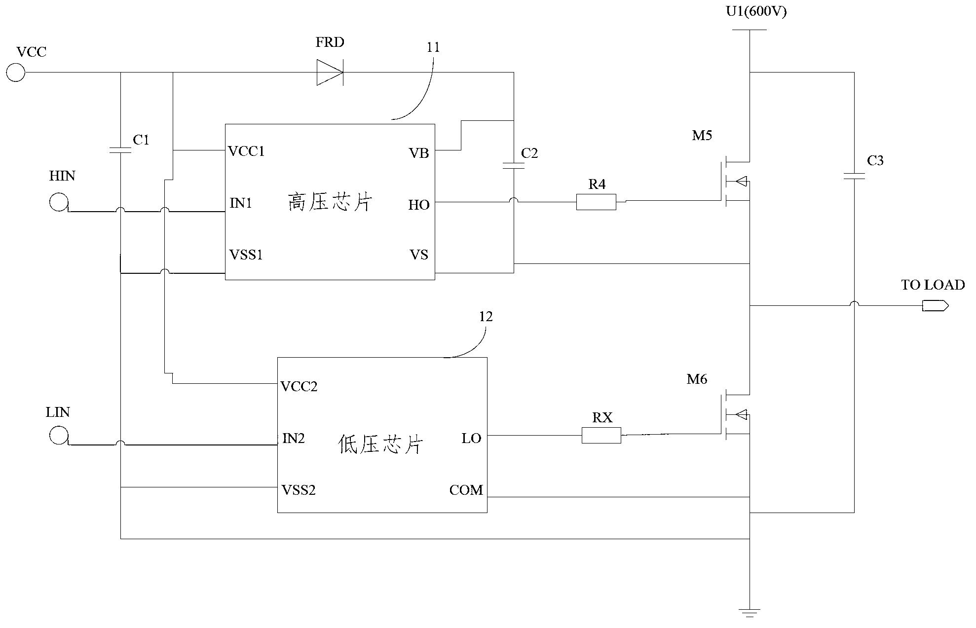
[0061] This embodiment proposes an integrated circuit, such as Figure 10 As shown, the integrated circuit includes a filter circuit 51, a narrow pulse generation circuit 52, a level shift circuit 53, a narrow pulse detection circuit 54, an output signal processing circuit 55 and a drive switch 56; the input terminal of the filter circuit 51 is connected to the input The signal VIN is connected, and the output terminal is connected to the input terminal of the narrow pulse generating circuit. The filter circuit 51 is the filter circuit of the integrated circuit described in the embodiment, and will not be described in detail here. The output end of the narrow pulse generation circuit 52 is connected to the input end of the level shift circuit 53, the output end of the level shift circuit 53 is connected to the input end of the narrow pulse detection circuit 54, and the narrow pulse The output end of the detection circuit 54 is connected to the input end of the output signal pr...


PUM


Abstract

The invention provides a filter circuit of an integrated circuit. The filter circuit of the integrated circuit comprises a low-level delay unit, a first filter unit, a high-level delay unit, a second filter unit and an RS trigger, wherein the input end of the low-level delay unit receives an input signal, the low-level delay unit is used for delaying and outputting the falling edge of the received input signal, the first filter unit is connected with the low-level delay unit and used for filtering a negative pulse with a pulse width smaller than the delay time of the low-level delay unit, the input end of the high-level delay unit receives the input signal, the high-level delay unit is used for delaying and outputting the rising edge of received input signal, the second filter unit is connected with the high-level delay unit and used for filtering a positive pulse with a pulse width smaller than the delay time of the high-level delay unit, the R input end of the RS trigger is connected with the output end of the second filter unit, and the S input end of the RS trigger is connected with the output end of the first filter unit. The filter circuit of the integrated circuit can filter pulses with smaller pulse widths. The invention further provides the integrated circuit.

Description

technical field [0001] The invention relates to the field of integrated circuits, in particular to an integrated circuit filter circuit and an integrated circuit. Background technique [0002] A high-voltage integrated circuit is a gate drive circuit with functions such as various protection circuits, low-voltage control circuits, and high-voltage power devices. It combines power electronics with semiconductor technology, which significantly improves the integration and stability of the whole machine. With the advantages of high integration density, small size, fast speed, and low power consumption, it gradually replaces traditional discrete devices, and is increasingly used in MOS (Metal-Oxide-SemiconductorField-Effect Transistor, Metal-Oxide-Semiconductor- field effect transistor) tube, IGBT (Insulated Gate Bipolar Transistor, insulated gate bipolar transistor) driving field. One of the cores of high-voltage integrated circuits is the level shift circuit. The function of ...

Claims


Application Information

Patent Timeline
IPC IPC(8): H03K19/007H03K3/013
Inventor 高存旗刘杰张华群
Owner 上海奔赛电子科技发展有限公司
Why Eureka
Try Eureka