A 3D printing-based packaging substrate and manufacturing method thereof

A packaging substrate, 3D printing technology, applied in printed circuit manufacturing, multi-layer circuit manufacturing, semiconductor/solid-state device manufacturing, etc. problem, to achieve good industrial applicability, reduce circuit loss and signal transmission delay effect

Inactive Publication Date: 2016-03-02
数驱技术有限公司
View PDF6 Cites 0 Cited by
  • Summary
  • Abstract
  • Description
  • Claims
  • Application Information

AI Technical Summary

Problems solved by technology

[0048] The wiring layer manufactured by powder spraying or droplet spraying has low precision, which is far from the requirements of high-density interconnection;
[0049] 2. The cost of nanomaterials is high
Unfortunately, due to historical reasons, the existing packaging substrate manufacturing technology adopts subtractive manufacturing technology, thus forming a huge and complex technical system and industrial chain

Method used


Image

  • A 3D printing-based packaging substrate and manufacturing method thereof
  • A 3D printing-based packaging substrate and manufacturing method thereof

Examples


Embodiment Construction

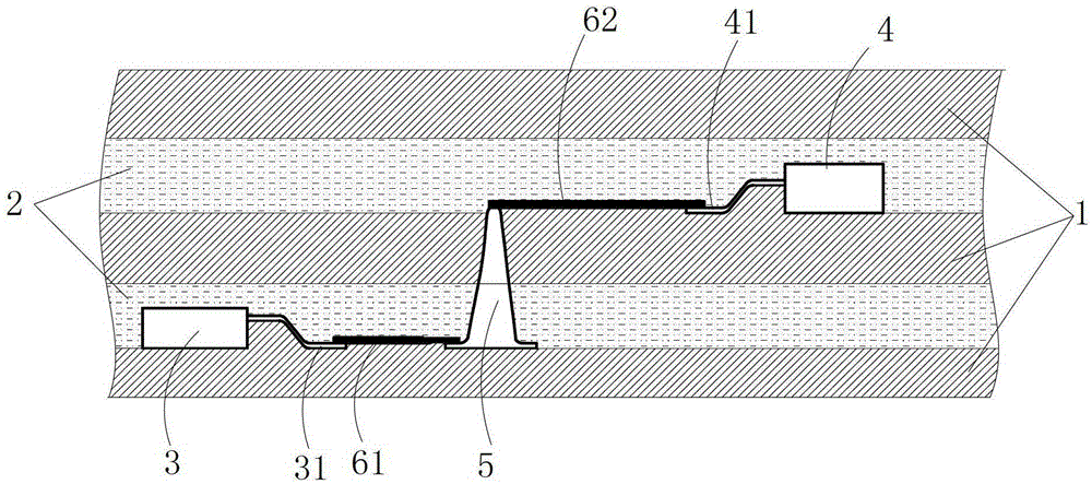
[0110] This application has been explained in the technical background, and the multilayer circuit board and the packaging substrate are no longer distinguished. This application regards a multilayer circuit board as a packaging substrate without embedded passive / active electronic devices. Therefore, in the present application, the packaging substrate includes a circuit board, especially a multilayer circuit board. Passive electronic devices include resistors, capacitors, inductors, etc. Active electronic devices include transistors, integrated circuits, chips and chip modules.

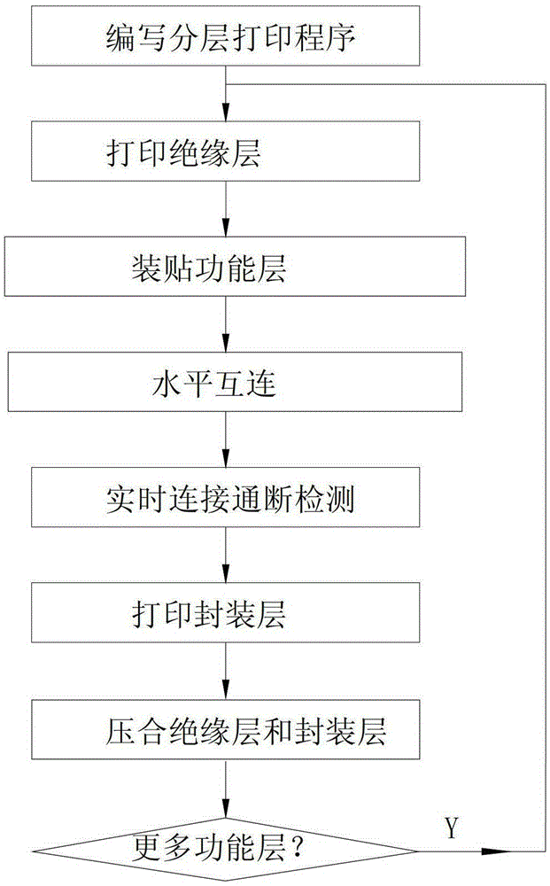
[0111] 3D printing technology has created a new concept of design and manufacturing.

[0112] One of the outstanding advantages of 3D printing technology is that it can realize parts made of functionally graded materials, and can directly manufacture parts with arbitrary complex structures. In particular, products that lose manufacturability due to complex three-dimensional structures inside, or pro...


PUM


Abstract

This application proposes a packaging substrate based on 3D printing and its manufacturing method, and re-examines the existing packaging substrate (multilayer circuit board) and its wiring layer manufacturing method. This application regards the main body of the packaging substrate (multilayer circuit board) as an insulating layer and packaging layer with a complex three-dimensional structure, and passive / active electronic devices and electronic connecting devices are embedded inside the packaging layer; , pads and their assemblies of different structures are regarded as electronic connection devices, and are treated equally with passive / active electronic devices and standardized. The technical solution of the present application cancels almost all the processes in the prior art of manufacturing the wiring layer, and changes the production method and manufacturing technology of the packaging substrate (multilayer circuit board).

Description

technical field [0001] This application belongs to the field of packaging substrate (Package Substrate) and circuit board (Printed Circuit Board, PCB) manufacturing, and specifically relates to the use of 3D printing technology to manufacture multilayer circuit boards, especially packaging substrates. technical background [0002] Printed circuit board or printed circuit board, also known as printed circuit board or printed circuit board, is referred to as circuit board in this application. [0003] As the mounting substrate of electronic devices, circuit boards are used for electrical connection and support of electronic devices. [0004] The multi-layer circuit board has a hierarchical structure, which consists of wiring layers (top layer, bottom layer, middle wiring layer), power layer (Power), ground layer (Ground), and auxiliary layers. The auxiliary layer includes the top solder mask layer and icon layer. (legend). [0005] The wiring layer is used to realize the ele...

Claims


Application Information

Patent Timeline
Patent Type & Authority Patents(China)
IPC IPC(8): H05K1/18H05K3/34H05K3/46H01L23/498
CPCH01L23/49822H01L21/4867H05K1/186H05K3/4664H01L2924/0002B33Y80/00H01L2924/00
Inventor 江俊逢吴柏江周丽
Owner 数驱技术有限公司
Why Eureka
Try Eureka