Packaging structure and preparation method thereof

A technology of packaging structure and rewiring structure, which is applied in the fields of semiconductor/solid-state device manufacturing, semiconductor/solid-state device components, semiconductor devices, etc. The effect of increasing the integration density

Pending Publication Date: 2021-06-04
SHANGHAI XIANFANG SEMICON CO LTD +1
View PDF12 Cites 0 Cited by
  • Summary
  • Abstract
  • Description
  • Claims
  • Application Information

AI Technical Summary

Problems solved by technology

[0004] Therefore, the technical problem to be solved by the present invention is to overcome the defect that the existing packaging structure cannot have high integration density and high-frequency transmission capability at the same time, so as to provide a packaging structure and its preparation method

Method used


Image

  • Packaging structure and preparation method thereof
  • Packaging structure and preparation method thereof
  • Packaging structure and preparation method thereof

Examples


preparation example Construction

[0043] On this basis, the present invention provides a method for preparing a packaging structure, comprising the following steps: providing a semiconductor substrate; etching the semiconductor substrate by using a high aspect ratio etching process, and forming a plurality of grooves in the semiconductor substrate groove; forming a conductive connection structure in the groove; forming a first rewiring structure, the first rewiring structure is located on one side of the semiconductor substrate and the conductive connection structure, and the first rewiring structure is connected to the conductive connection structure The conductive connection structure is connected; after the first rewiring structure is formed, the semiconductor substrate is removed. The packaging structure obtained by the above preparation method can simultaneously have higher integration density and high-frequency transmission capability.

[0044] The technical solutions of the present invention will be cle...

Embodiment 1

[0047] see figure 1 , the invention provides a method for preparing a packaging structure, comprising the following steps:

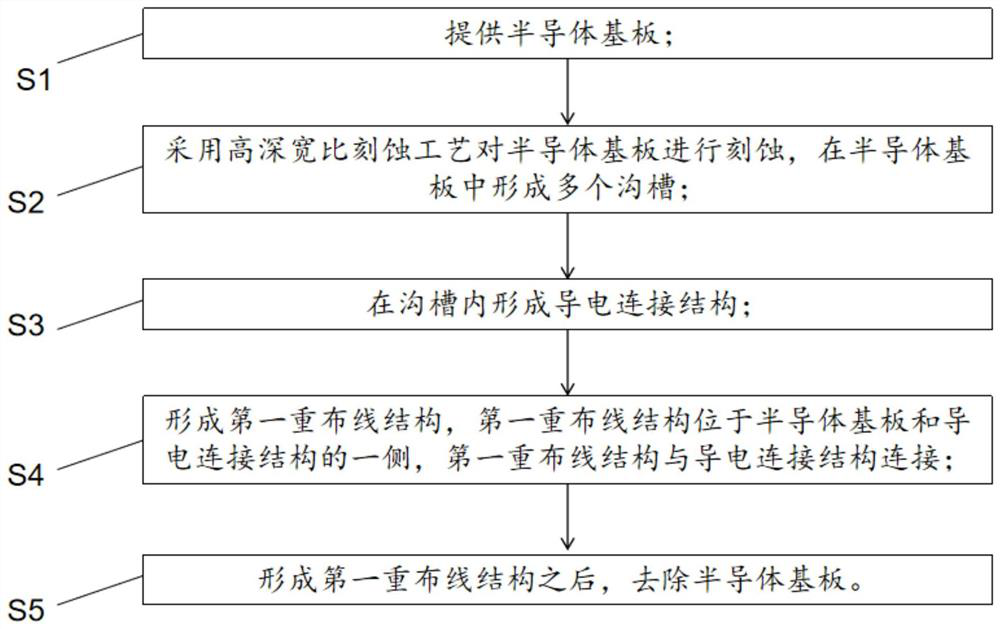
[0048] S1, providing a semiconductor substrate 1;

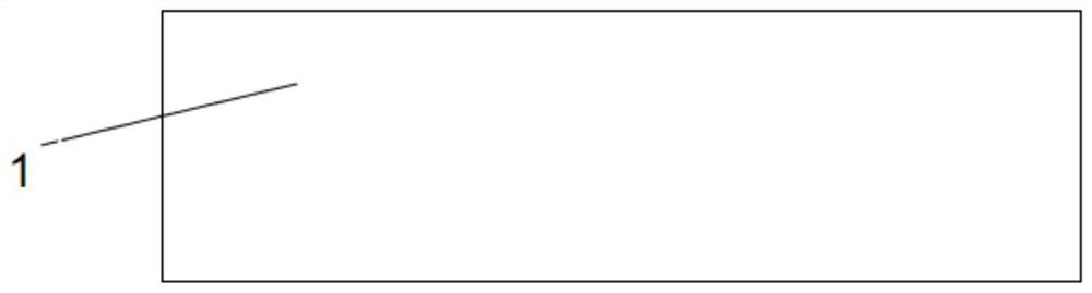
[0049] S2. Etching the semiconductor substrate 1 by using a high aspect ratio etching process to form a plurality of trenches 2 in the semiconductor substrate 1;

[0050] S3, forming a conductive connection structure 3 in the trench 2;

[0051] S4, forming a first rewiring structure 4, the first rewiring structure 4 is located on one side of the semiconductor substrate 1 and the conductive connection structure 3, the first rewiring structure 4 is connected to the conductive connection structure 3 connect;

[0052] S5. After the first rewiring structure 4 is formed, the semiconductor substrate 1 is removed.

[0053] In the preparation method of the above packaging structure, the semiconductor substrate is etched by a high aspect ratio etching process, a conductive connection structure is formed in th...

Embodiment 2

[0081] This embodiment provides a method for preparing a package structure, which differs from the method for preparing a package structure provided in Example 1 in that:

[0082] see Figure 16 , after the trench 2 is formed in step S2, a dielectric layer 12 is formed on the inner wall of the trench 2, so that after the conductive connection structure 3 is formed in step S3, as Figure 17 As shown, the dielectric layer 12 on the inner wall of the trench 2 is located between the conductive connection structure 3 and the semiconductor substrate 1, so that after the second encapsulation layer 9 is formed, as Figure 18 As shown, the second encapsulation layer 9 wraps the dielectric layer 12 outside the conductive connection structure 3 . Since the bonding force between the dielectric layer and the second encapsulation layer is greater than the bonding force between the conductive connection structure and the second encapsulation layer, the bonding stability of the second encaps...


PUM


Abstract

The invention provides a packaging structure and a preparation method thereof. The preparation method comprises the following steps: providing a semiconductor substrate; etching the semiconductor substrate by adopting a high aspect ratio etching process, and forming a plurality of grooves in the semiconductor substrate; forming a conductive connection structure in the groove; forming a first rewiring structure, wherein the first rewiring structure is located on one side of the semiconductor substrate and the conductive connection structure, and the first rewiring structure is connected with the conductive connection structure; after the first redistribution structure is formed, removing the semiconductor substrate. The packaging structure prepared by the preparation method has relatively high integration density and high-frequency transmission capability at the same time.

Description

technical field [0001] The invention relates to the technical field of semiconductor packaging, in particular to a packaging structure and a preparation method thereof. Background technique [0002] With the development of electronic technology, semiconductor packaging tends to develop in the direction of high density, multi-function, low power consumption and miniaturization. Fan-out wafer-level packaging technology can perform vertical and horizontal multi-chip heterogeneous integration in one package structure, and has a high degree of integration flexibility. In the existing fan-out wafer-level packaging technology, the methods of forming through plastic vias (TMV) for the vertical interconnection of the three-dimensional fan-out package and the antenna-integrated fan-out package include laser hole burning, vertical wire bonding, and thick photolithography. Glue plating or cladding layer punching. [0003] However, since the package structure obtained by the above meth...

Claims


Application Information

Patent Timeline
Patent Type & Authority Applications(China)
IPC IPC(8): H01L21/56H01L23/31H01L21/60H01L23/488
CPCH01L23/3128H01L21/56H01L24/02H01L24/11H01L24/13H01L2224/13008H01L2224/111H01L2224/02331H01L2224/02333H01L2224/02381H01L2224/02379
Inventor 王全龙曹立强严阳阳戴风伟
Owner SHANGHAI XIANFANG SEMICON CO LTD
Why Eureka
Try Eureka