Semiconductor memory device and manufacturing method thereof

A technology for storage devices and manufacturing methods, which is applied in semiconductor/solid-state device manufacturing, semiconductor devices, semiconductor/solid-state device components, etc., and can solve the problem of long transmission paths of non-volatile memory chips, bandwidth limitations of chip interface transmission lines, and data interaction Speed ​​limitation and other issues, to achieve the effect of reducing the length of the I/O connection, saving the circuit area, and reducing the area

Pending Publication Date: 2021-03-02
CHANGXIN MEMORY TECH INC
View PDF0 Cites 0 Cited by
  • Summary
  • Abstract
  • Description
  • Claims
  • Application Information

AI Technical Summary

Problems solved by technology

The disadvantage of this situation is that the transmission path between the volatile memory chip and the non-volatile memory chip is long, and there are bandwidth limitations in the chip interface and transmission lines, the speed of data interaction is limited, and the overall size is too large, so it is difficult to adapt to the needs. Highly integrated applications

Method used


Image

  • Semiconductor memory device and manufacturing method thereof
  • Semiconductor memory device and manufacturing method thereof
  • Semiconductor memory device and manufacturing method thereof

Examples


Embodiment Construction

[0035] A specific implementation of a semiconductor storage device and a manufacturing method thereof provided by the present invention will be described in detail below with reference to the accompanying drawings.

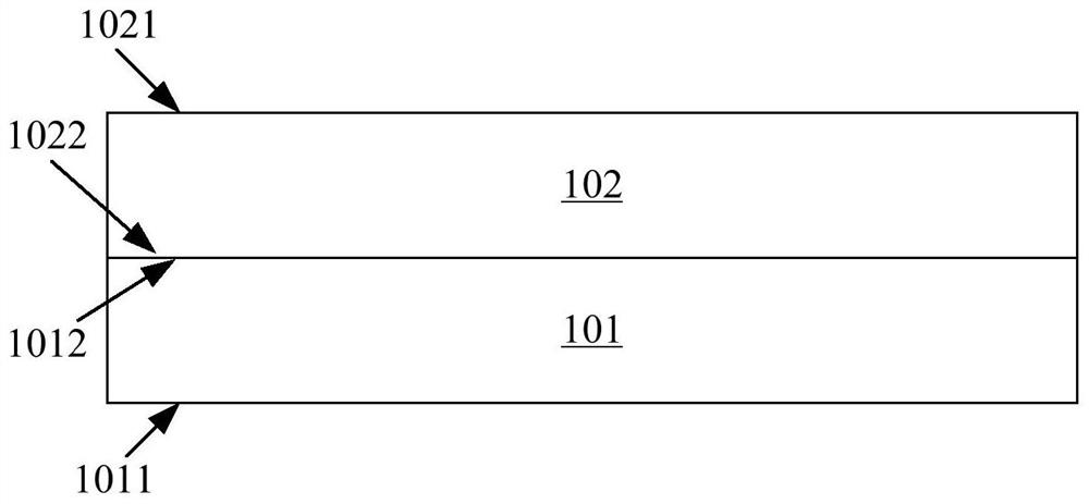
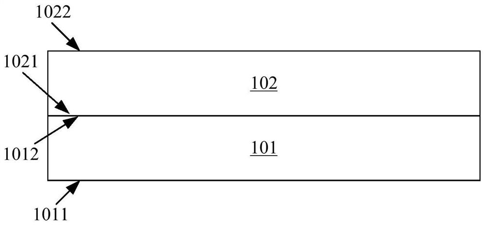
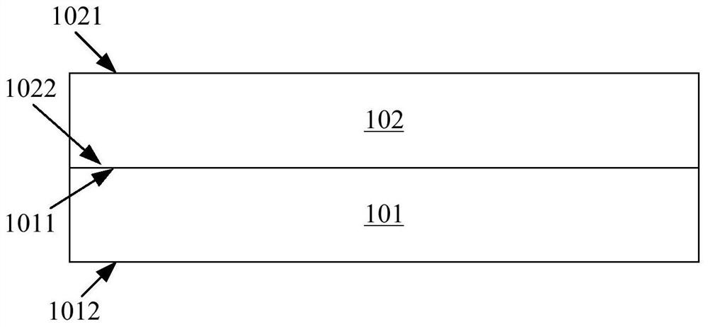
[0036] Please refer to FIG. 1 , which is a schematic structural diagram of a semiconductor storage device according to an embodiment of the present invention.

[0037] The semiconductor storage device in this specific embodiment includes: a first storage chip 101 and a second storage chip 102, and the first storage chip 101 and the second storage chip 102 are stacked and connected.

[0038] The first memory chip 101 and the second memory chip 102 may be different types of memory chips respectively. In a specific implementation manner, the first memory chip 101 is a volatile memory chip, and the second memory chip 102 is a non-volatile memory chip. In this specific implementation manner, the first storage chip 101 is a DRAM chip, and the second storage chip 102 is...


PUM


Abstract

The invention discloses a semiconductor memory device and a manufacturing method thereof. The semiconductor memory device includes: a first memory chip in which a first memory array is formed; and a second storage array formed in the second storage chip. The back surface of the second storage chip is stacked on the surface of the first storage chip; a second conductive column penetrating through the second storage chip is formed in the second storage chip, and the second storage chip is electrically connected with the first storage chip through the second conductive column; a peripheral circuit is formed in the first memory chip, the peripheral circuit comprises a first circuit, at least part of a second circuit and a common circuit, the first circuit is used for controlling the first memory array, the second circuit is used for controlling the second memory array, the first circuit is connected with the first memory array, and the second circuit is connected with the second memory array; and the common circuit connects the first circuit and the second circuit. The data transmission efficiency of the semiconductor memory device is improved.

Description

technical field [0001] The invention relates to the technical field of integrated circuits, in particular to a semiconductor storage device and a manufacturing method thereof. Background technique [0002] Because volatile memory chips (such as DRAM) have faster read speeds, and non-volatile memory chips (such as NAND flash) have the advantage of not losing data when power is turned off, most modern data processing systems need to include volatile memory chips at the same time. Memory chips and non-volatile memory chips to take advantage of their respective advantages. Since the structures of the volatile memory chips and the non-volatile memory chips are different, they are usually manufactured using different processes and each forms an independent chip. [0003] When the data processing system includes both a volatile memory chip and a non-volatile memory chip, the two memory chips usually exist independently and are connected to each other through a transmission line fo...

Claims


Application Information

Patent Timeline
Patent Type & Authority Applications(China)
IPC IPC(8): H01L25/065H01L23/48H01L21/768H01L21/60
CPCH01L25/0657H01L23/481H01L24/81H01L21/76898H01L2224/8136H01L2224/48091H01L2224/16145H01L2924/00014
Inventor 朱一明平尔萱
Owner CHANGXIN MEMORY TECH INC
Why Eureka
Try Eureka