OLED (Organic Light Emitting Diode) panel thinning device and application method thereof

A panel and partition technology, applied in the field of OLED panel thinning devices, can solve problems such as misjudgment of OLED device qualification, influence on process stability, and deviation of measurement results, and achieve simple and clear methods of use, easy promotion and application, The effect of ensuring stability

Inactive Publication Date: 2013-10-02
SICHUAN CCO DISPLAY TECH
View PDF5 Cites 2 Cited by
  • Summary
  • Abstract
  • Description
  • Claims
  • Application Information

AI Technical Summary

Problems solved by technology

The disadvantage of using this method is that it is difficult to completely remove the silica gel in the later stage, and the current detection accuracy of OLED is at the nanoampere level. Under such high-precision measurement conditions, extremely small residual glue particles can also cause serious deviations in the measurement results. , resulting in a misjudgment of whether the OLED device is qualified or not, affecting the setting of process parameters in the previous process, and thus affecting the stability of the entire process

Method used


Image

  • OLED (Organic Light Emitting Diode) panel thinning device and application method thereof
  • OLED (Organic Light Emitting Diode) panel thinning device and application method thereof
  • OLED (Organic Light Emitting Diode) panel thinning device and application method thereof

Examples


Embodiment Construction

[0035] In order to make the object, technical solution and advantages of the present invention clearer, the present invention will be further described in detail below in conjunction with the accompanying drawings and embodiments. It should be understood that the specific embodiments described here are only used to explain the present invention, not to limit the present invention.

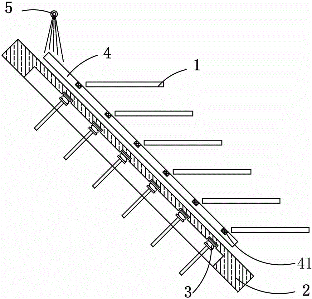
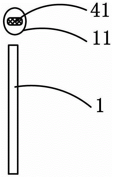
[0036] Such as figure 1 As shown, the OLED panel thinning device in this embodiment includes an etching solution spray system, and also includes a nitrogen nozzle 1, a quartz partition 2 and a constant temperature heater 3, and the nitrogen nozzle 1 and the OLED panel 4 The upper surface forms an included angle of 45° to 50° and the distance between the nitrogen nozzle 1 and the upper surface of the OLED panel 4 is 0.5 to 1.5 times the length of the major axis of the oval detection hole of the reserved electrode. The included angle is set such that The direction of the nitrogen gas flow is opposit...


PUM


Abstract

The invention discloses an OLED (Organic Light Emitting Diode) panel thinning device which comprises an etching liquid spraying system as well as nitrogen ejection tubes, quartz baffles and constant temperature heaters, wherein an inclined angle is formed between the nitrogen ejection tubes and the upper surface of an OLED panel and the nitrogen ejection tubes are not contacted with the OLED panel; one nitrogen ejection tube is arranged in the position of each preserved electrode testing hole in the OLED panel; the quartz baffles are arranged on the back side of the OLED panel in parallel; mounting holes of which the positions correspond to the positions of the preserved electrode testing holes in the OLED panel are formed in one sides opposite to the OLED panel, in the quartz baffles; the constant temperature heaters are arranged inside the mounting grooves; a spraying tube of the etching liquid spraying system is positioned above the OLED panel and is not contacted with the OLED panel. The invention further discloses an application method of the OLED panel thinning device. The OLED panel thinning device is simple in structure, no impurities are introduced in the application process, the misjudgement on whether the OLED panel is qualified or not is avoided, the operation is simple and convenient, and the application is convenient.

Description

technical field [0001] The invention belongs to the technical field of organic electroluminescence display, and in particular relates to an OLED panel thinning device and a use method thereof. Background technique [0002] The continuous development of smartphones and tablets requires lighter and thinner displays. Limited by the manufacturing process, the thickness of the glass substrate can no longer be made thinner. Therefore, whether it is a liquid crystal panel or an OLED panel, the panel can only be thinned to achieve a lighter and thinner panel after alignment bonding or packaging is completed. Quality requirements. Compared with the thinning of liquid crystal panels, OLED panels are more difficult to manufacture during the thinning process, because during the thinning process of OLED panels, the reserved detection electrodes of OLED devices are easily corroded by etching solution, resulting in damage. At present, when the OLED panel is etched and thinned, the usual...

Claims


Application Information

Patent Timeline
Patent Type & Authority Applications(China)
IPC IPC(8): C03C15/00
Inventor 向欣任海成洛贤夏维高
Owner SICHUAN CCO DISPLAY TECH
Why Eureka
Try Eureka