Atom trapping and optical latticing method for chip surface

A technology of surface optics and surface plasmon, applied in the field of cold atom laser trapping and cold atom optical lattice, laser trapping and cold atom optic lattice, can solve problems such as deficiencies

Inactive Publication Date: 2013-10-02
JIANGSU UNIV
View PDF0 Cites 11 Cited by
  • Summary
  • Abstract
  • Description
  • Claims
  • Application Information

AI Technical Summary

Problems solved by technology

[0003] Although great achievements have been made in the study of atomic trapping and optical lattices on solid surfaces, due to the influence of the diffraction limit of light, the characteristic scale of the light field of traditional atomic trapping and optical lattices is generally limited to half-wavelength. Therefore, this will bring some shortcomings to the basic research of atomic trapping on solid surfaces and atomic optical lattices

Method used


Image

  • Atom trapping and optical latticing method for chip surface
  • Atom trapping and optical latticing method for chip surface

Examples


Embodiment 1

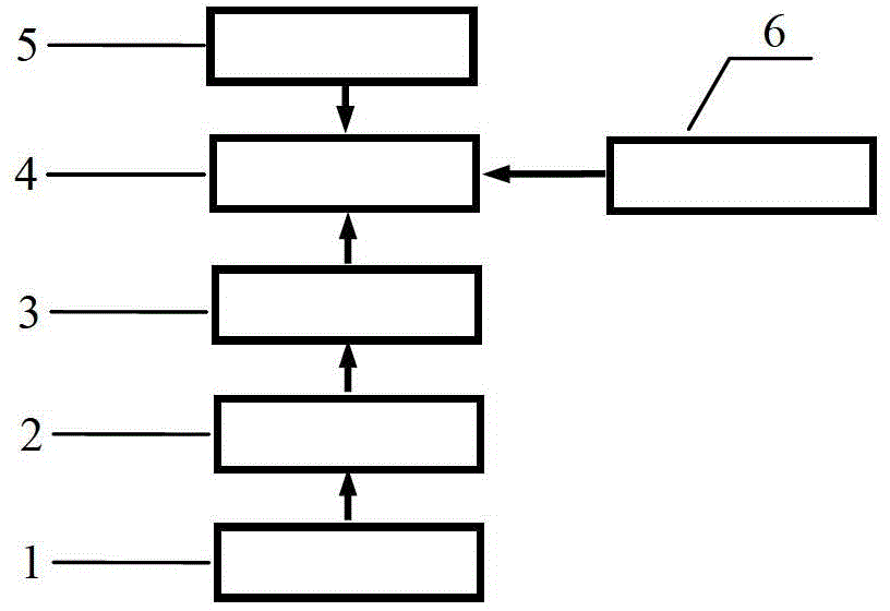
[0023] (1) Using the finite difference time domain method (FDTD) to determine figure 1 The structural parameters of the coated inverted pyramid prism 4 which can realize atom trapping and surface optical lattice.

[0024] (2) Process the glass material (such as fused quartz) into an inverted pyramid prism by rough grinding, fine grinding, polishing and other processing procedures, and then use magnetron sputtering to coat a layer of precious metal on the bottom of the inverted pyramid prism (such as Select silver) thin film, process out figure 1 Coated inverted pyramid prisms in 4.

[0025] (3) Use the bracket to place figure 1 The coated inverted pyramid prism 4 is placed in the laser optical path system, installed and fixed in place, and the coated surface is required to be placed in parallel.

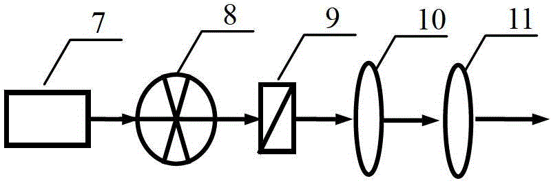
[0026] (4) figure 1 Medium light source system 1 consists of figure 2 The laser 7, the chopper 8, the polarizer 9, the focusing lens 10 and the beam expanding lens 11 are compo...


PUM


Abstract

The invention discloses an atom trapping and optical latticing method for a chip surface, and relates to the field of neutral cold atom laser trapping and optical latticing. According to the method, the side surface of a coated inverted pyramid lens with an upward coated surface is irradiated by laser, evanescent waves generated by total reflection of the side surface of the lens are excited on the surface of a metal film to generate near-field surface plasmon polaritons, and loaded neutral cold atoms are subjected to effective trapping, one-dimensional atom surface optical latticing and two-dimensional atom surface optical latticing by the near-field surface plasmon polaritons and the interference light fields of the polaritons. The method can be used for achieving chip surface tom trapping and atom surface optical latticing of different types of neutral cold atoms, and is simple in principle, convenient to operate and wide in application range.

Description

technical field [0001] The invention relates to the field of cold atom laser trapping and cold atom optical lattice, in particular to a kind of cold atom laser trapping and cold atom optical lattice for near-field optics on the surface of a chip, which is suitable for near-field optics on the chip surface of any type of neutral cold atoms Laser-trapped and cold-atom optical lattices. Background technique [0002] In recent years, the trapping of neutral cold atoms on solid surfaces and the study of optical lattices have become one of the research hotspots in the field of cold atom physics and atomic optics. It is very important in the research of quantum information, optical lattices and atomic chips. Significance. This technology has been gradually applied to the confinement and control of cold atoms and Bose-Einstein condensates (BEC), quantum transmission and tunneling, and the miniaturization and integration of quantum solid-state systems. Utilizing the evanescent wave...

Claims


Application Information

Patent Timeline
Patent Type & Authority Applications(China)
IPC IPC(8): G21K1/00
Inventor 王正岭王艳丽姜文帆
Owner JIANGSU UNIV
Why Eureka
Try Eureka