

Metal capacitor for all-directional connection and layout method
A metal capacitor and wiring method technology, applied in circuits, electrical components, electrical solid devices, etc., can solve the problems of ignoring the mutual influence of the upper and lower metal layers, reducing the efficiency of metal capacitors, sacrificing the capacitance value, etc., to reduce the layout workload and increase. Large metal capacitor, the effect of eliminating circuit noise
- Summary
- Abstract
- Description
- Claims
- Application Information
AI Technical Summary
Problems solved by technology
Method used
Image

Examples
Embodiment Construction
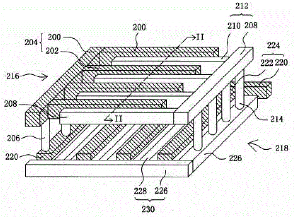
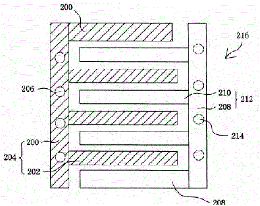
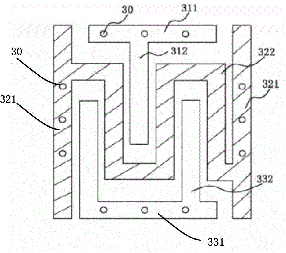
[0032] The metal capacitor with omnidirectional connection disclosed by the present invention draws on the form of the finger capacitor in the prior art to first form a unit module of a metal capacitor, including two layers of finger capacitors on an odd-numbered layer and an even-numbered layer. image 3 It is a schematic diagram of odd-numbered layer capacitance of the present invention, Figure 4 It is a schematic diagram of the even-numbered layer capacitor of the present invention, the odd-numbered layer and the even-numbered layer respectively include an upper part and a lower part, the upper part is T-shaped, and the lower part is U-shaped.
[0033] The upper and lower parts of the odd-numbered layers respectively include horizontal traces 311 and a plurality of fingers 312, and the fingers are staggered up and down, and a continuous serpentine trace 322 is also included between the fingers staggered up and down, as shown in the figure The hatched portion of the oblique...
PUM
 Abstract
Description
Claims
Application Information