Patterned substrate manufacturing method

A technology of patterned substrates and fabrication methods, applied in electrical components, circuits, semiconductor devices, etc., can solve the problems of pattern splicing part deformation, affecting HBLED luminous efficiency, exposure field splicing error, etc.

Inactive Publication Date: 2013-10-02
SHANGHAI UNIV
View PDF8 Cites 15 Cited by
  • Summary
  • Abstract
  • Description
  • Claims
  • Application Information

AI Technical Summary

Problems solved by technology

However, due to the special arrangement of PSS graphics, splicing errors will occur between the exposure fields of view, and the spliced ​​parts of the patterns will be deformed, which will eventually affect the luminous efficiency of HBLEDs.

Method used


Image

  • Patterned substrate manufacturing method
  • Patterned substrate manufacturing method
  • Patterned substrate manufacturing method

Examples


Embodiment Construction

[0022] Preferred embodiments of the present invention are described in detail as follows in conjunction with accompanying drawings:

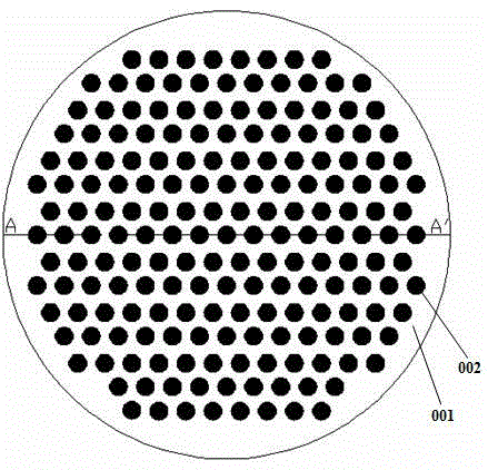
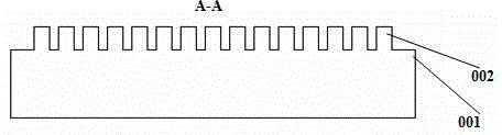
[0023] figure 1 A schematic plan view of a PSS fabricated on a sapphire substrate for one embodiment of the present invention. exist figure 1 In the schematic diagram of the patterned substrate shown, 001 is a non-patterned substrate area, and 002 is a patterned substrate area. In order to better illustrate the structure of the temperature resistance sensor, a schematic cross-sectional structure diagram of the above-mentioned sensor in the A-A' direction is made, as figure 2 shown.

[0024] figure 2 for figure 1 The shown schematic diagram of the cross-sectional structure of the patterned substrate structure along the direction A-A in the figure. from figure 2 It can be seen that 001 is the etched area, and 002 is the unetched area.

[0025] Those skilled in the art should recognize that the above-mentioned figure 1 with figure 2 T...


PUM


Abstract

The invention relates to a patterned substrate manufacturing method. The method comprises the following steps: defining a pattern zone of a part of patterned substrate on the front surface of a substrate by using the photoetching technology; then depositing a barrier layer on the front surface of the substrate, and using the lift-off process to strip photoresist so as to leave the barrier layer on the surface of the substrate; performing the photoetching technology again to define a pattern zone of the remaining part of the patterned substrate; then depositing the other barrier layer on the front surface of the substrate, and using the lift-off process to strip the photoresist so as to leave the barrier layer on the surface of the substrate; finally performing the dry or wet etching process to form a patterned substrate. By the method provided by the invention, the problem that the luminous efficiency of an HBLED (High Brightness Light Emitting Diode) is affected by splicing errors among exposure fields and deformation of pattern splicing part is solved.

Description

technical field [0001] The invention relates to the technical field of high-brightness light-emitting diode (HBLED) manufacturing, in particular, the invention relates to a patterned substrate manufacturing method. Background technique [0002] In the processing technology of high-brightness light-emitting diode HBLED, a patterned substrate (PSS) prepared on a sapphire substrate is required. PSS can reduce the lattice mismatch between the epitaxial material (GaN) and the sapphire substrate material. Lattice mismatch will reduce the carrier generation rate, generate a lot of heat energy, and shorten the life of the chip. In addition, PSS also has the effect of enhancing light reflection efficiency, so it is currently the mainstream technology for improving the luminous efficiency of HBLED. [0003] The process flow of PSS is to first deposit a barrier layer on the sapphire substrate; then apply photoresist, and use photolithography to make periodic patterns on the sapphire ...

Claims


Application Information

Patent Timeline
Patent Type & Authority Applications(China)
IPC IPC(8): H01L33/00H01L33/22
Inventor 唐世弋李冬梅程经纬程涛王刚
Owner SHANGHAI UNIV
Why Eureka
Try Eureka