Metal microcavity optical coupling terahertz quantum well photon detector

A photon detector, quantum well technology, applied in semiconductor devices, electrical components, circuits, etc., can solve the problems of low responsivity and low operating temperature, and achieve the effects of improving responsivity, strong practicability, and simple structure

Active Publication Date: 2013-10-23
SHANGHAI INST OF MICROSYSTEM & INFORMATION TECH CHINESE ACAD OF SCI
View PDF3 Cites 11 Cited by
  • Summary
  • Abstract
  • Description
  • Claims
  • Application Information

AI Technical Summary

Problems solved by technology

[0005] In view of the above-mentioned shortcoming of the prior art, the object of the present invention is to provide a metal microcavity optically coupled terahertz q

Method used


Image

  • Metal microcavity optical coupling terahertz quantum well photon detector
  • Metal microcavity optical coupling terahertz quantum well photon detector
  • Metal microcavity optical coupling terahertz quantum well photon detector

Examples


Embodiment 1

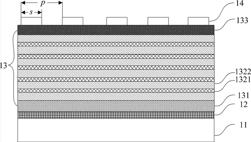
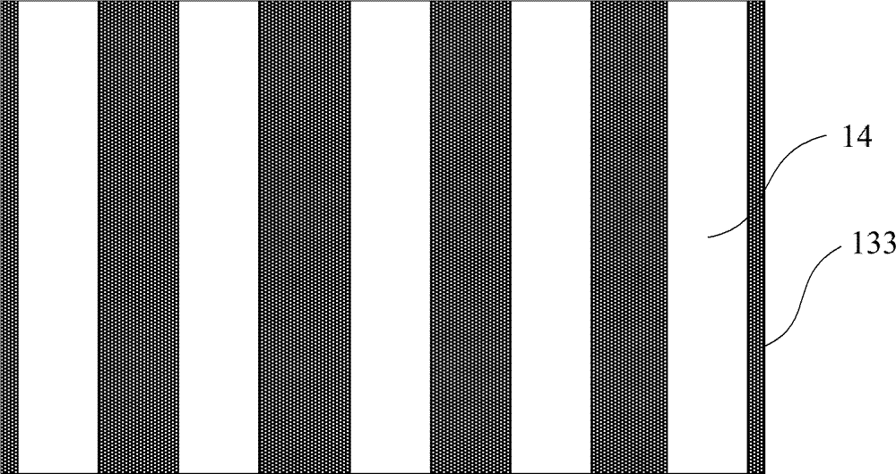
[0032] see Figure 1a ~ Figure 4 , as shown in the figure, the present invention provides a metal microcavity optically coupled terahertz quantum well photon detector, at least including: a semiconductor substrate 11; a metal reflective layer 12, combined with the semiconductor substrate 11; a multi-quantum well structure 13, comprising the lower electrode 131 combined with the metal reflective layer 12, the GaAs / (Al, Ga)As quantum well stacks 1321 and 1322 combined with the lower electrode 131, and the GaAs / (Al, The upper electrode 133 of the Ga) As quantum well stack 1321 and 1322; the metal grating 14, combined with the multi-quantum well structure 13, includes a plurality of metal strips arranged at intervals; the metal grating 14, the multi-quantum well structure 13 and the The metal reflective layer 12 forms a metal resonant microcavity of Fabry-Perot structure.

[0033] In this embodiment, the semiconductor substrate 11 is a GaAs substrate, of course, in other embodime...

Embodiment 2

[0047] see Figure 1a ~ Figure 4 , as shown in the figure, the present invention provides a metal microcavity optically coupled terahertz quantum well photon detector, at least including: a semiconductor substrate 11; a metal reflective layer 12, combined with the semiconductor substrate 11; a multi-quantum well structure 13, comprising the lower electrode 131 combined with the metal reflective layer 12, the GaAs / (Al, Ga)As quantum well stacks 1321 and 1322 combined with the lower electrode 131, and the GaAs / (Al, The upper electrode 133 of the Ga) As quantum well stack 1321 and 1322; the metal grating 14, combined with the multi-quantum well structure 13, includes a plurality of metal strips arranged at intervals; the metal grating 14, the multi-quantum well structure 13 and the The metal reflective layer 12 forms a metal resonant microcavity of Fabry-Perot structure.

[0048] In this embodiment, the semiconductor substrate 11 is a GaAs substrate. The material of the metal r...


PUM

PropertyMeasurementUnit
Widthaaaaaaaaaa
Thicknessaaaaaaaaaa
Widthaaaaaaaaaa

Abstract

The invention provides a metal microcavity optical coupling terahertz quantum well photon detector, which comprises a semiconductor substrate, a metal reflective layer, a multi-quantum well structure and a metal grating, wherein the metal grating, the multi-quantum well structure and the metal reflective layer form a metal resonant microcavity with a Fabry-Perot structure, incident photons are enabled to form a resonant mode conforming to the Fabry-Perot structure in the cavity through adjusting the period of the metal grating, the width of a metal strip and the thickness of the multi-quantum well structure, and a strong field region is formed in the metal resonant microcavity, thereby improving the effective strength of incident light, and improving the response rate, the detection sensitivity and the working temperature of the device. The metal microcavity optical coupling terahertz quantum well photo detector has the advantages of simple structure, obvious effect, strong practicability, and is applicable to industrial production.

Description

technical field [0001] The invention belongs to the field of semiconductors, in particular to a metal microcavity optically coupled terahertz quantum well photon detector. Background technique [0002] Quantum well detector is an important detector working in the mid-to-far infrared and terahertz frequency bands. Terahertz quantum well detector is a photon-type detector with important application prospects in the terahertz frequency band, which has the characteristics of high sensitivity, fast detection speed and narrow-band response. The main structure of this detector includes upper contact layer, multi-quantum well layer and lower contact layer. The number of quantum wells is between 10 and 100, and the thickness of the device is between 2.0 and 5.0 μm in the growth direction of the quantum wells. The bound electrons are introduced into the quantum well by doping. Due to the parabolic energy dispersion relationship, these bound electrons can only absorb photons with an ...

Claims


Application Information

Patent Timeline
IPC IPC(8): H01L31/0232H01L31/0352H01L31/101
Inventor 郭旭光曹俊诚张戎张真真谭智勇
Owner SHANGHAI INST OF MICROSYSTEM & INFORMATION TECH CHINESE ACAD OF SCI
Why Eureka
Try Eureka