Supercharge Your Innovation With Domain-Expert AI Agents!

A control method for line scan chip for improving plasma display emi low frequency exceeding standard

A plasma display, chip control technology, applied in static indicators, instruments, etc., can solve the problems of slow opening, impossible to achieve high-voltage concurrent operation of line scan chips, EMI, etc., to increase current capacity, reduce EMI radiation, and accelerate the surface. effect of electric field

Active Publication Date: 2016-06-15
SICHUAN CHANGHONG ELECTRIC CO LTD
View PDF4 Cites 0 Cited by
  • Summary
  • Abstract
  • Description
  • Claims
  • Application Information

AI Technical Summary

Problems solved by technology

If the high voltages of 768 lines are all converted from low level to high level during concurrent actions, the superposition of about 300mA current in each line will result in a current of about 230A. If the output of the line scanning chip is not controlled concurrently, it will be impossible. Realize the high-voltage concurrent operation of the line scanning chip; since the output stage of the line scanning chip uses LIGBT (Lateral Insulated Gate Bipolar Transistor), the closing process is much slower than the opening process due to the high minority carrier injection concentration of LIGBT itself during the closing process , the turn-on process of the power tube is affected by the driving ability of its gate electrode. The gate of the power tube can be regarded as a capacitor. When the charge reaches the threshold voltage, the channel region of the power tube is opened, and the current at the moment of turn-on is relatively large. Its di / dt can cause serious EMI problem, and this is the deficiency that existing technology exists

Method used


Image

  • A control method for line scan chip for improving plasma display emi low frequency exceeding standard

Examples


Embodiment Construction

[0014] In order to clearly illustrate the technical characteristics of this solution, the following describes this solution through a specific implementation mode combined with its accompanying drawings.

[0015] The control method of this program is:

[0016] a. When the line scanning chips operate concurrently, the 96 output channels of the line scanning chips are grouped;

[0017] b. The 96 output channels are divided into 4 groups, 24 in each group, the delay between the first group and the second group is 40ns, the delay between the second group and the third group is 60ns, and the delay between the third group and the fourth group The delay is 50ns;

[0018] c. Add a clamp tube and a PN junction capacitance to the low-voltage tube input end of the line scan chip.

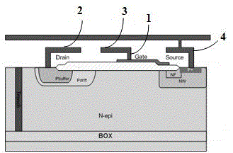
[0019] The output stage of the line scanning chip adopts the PLDMOS transistor of the gate field plate structure.

[0020] In the present invention, firstly, when concurrent operation of row scanning chips ...


PUM


Abstract

The invention provides a technical scheme related to a row scanning chip control method for improving plasma display EMI low frequency excess. According to the scheme, packet control performed on the output end of a row scanning chip is used, meanwhile, a clamper tube and a PN junction capacitor are added to the input end of a low-voltage tube, and therefore EMI radiation caused by high voltage power supply large current brought by punchthrough can be effectively reduced in a high-voltage concurrent movement process of the row scanning chip.

Description

technical field [0001] The present invention relates to a control method for reducing the influence of display low-frequency radiation, especially a control method for row-scanning chips to improve plasma display EMI low-frequency exceeding the standard. Background technique [0002] In the prior art, the known technology is that in the three-electrode driven plasma display module, the PDP line scanning chip is used to drive the Y electrodes of the display unit of the plasma module, and output addressing high-voltage pulses. Cooperate with the addressing A electrode in rows or interlaced rows to form a voltage greater than 200V to discharge the display unit to obtain wall charges, and then conduct cyclic discharge through the X and Y electrodes to form a certain duration to determine the gray level, through the gray level and silver light The color combination of powder forms a colorful picture. [0003] Taking a plasma display with 768 lines as an example, 8 line scanning ...

Claims


Application Information

Patent Timeline
Patent Type & Authority Patents(China)
IPC IPC(8): G09G3/28
Inventor 孙镇黄勇黄光佐梁涛
Owner SICHUAN CHANGHONG ELECTRIC CO LTD
Features
  • R&D
  • Intellectual Property
  • Life Sciences
  • Materials
  • Tech Scout
  • Unparalleled Data Quality
  • Higher Quality Content
  • 60% Fewer Hallucinations
Learn More