Supercharge Your Innovation With Domain-Expert AI Agents!

Method for forming stress layer in stress memorization technique

A stress memory technology and stress layer technology, applied in the field of semiconductor manufacturing, can solve problems affecting the deposition of stress layers, uneven stress, unfavorable ion implantation process, etc.

Active Publication Date: 2013-10-30
SEMICON MFG INT (SHANGHAI) CORP
View PDF4 Cites 6 Cited by
  • Summary
  • Abstract
  • Description
  • Claims
  • Application Information

AI Technical Summary

Problems solved by technology

In the actual application of SMT technology manufacturing process, such as figure 1 As shown, when forming the stress layer 7, such as a silicon nitride layer with tensile stress, due to the shrinkage of the overall feature size of PMOS1 and NMOS2, the distance between the PMOS gate 3 and the NMOS gate 4 is also reduced, and due to The gates 3 and 4 are respectively formed with gate sidewalls 5 and 6, so that as the adjacent PMOS and NMOS gate structures are too close, the deposition rate of the stress layer 7 at the corner position of the adjacent gate structure is greater than The deposition rate at other positions, therefore, will cause the stress layer 7 formed at the corners of the adjacent PMOS and NMOS transistor gate structures to be too thick, and affect the deposition of the stress layer between the PMOS and NMOS transistor gate structures, thereby causing Appears between adjacent PMOS and NMOS gates as figure 1 The void A shown in the figure will lead to uneven stress in the subsequent process and affect the performance of the device. If only the width of the gate sidewall layer in the gate structure is reduced, it will have an adverse impact on the subsequent ion implantation process.

Method used


Image

  • Method for forming stress layer in stress memorization technique
  • Method for forming stress layer in stress memorization technique
  • Method for forming stress layer in stress memorization technique

Examples


Embodiment Construction

[0028] In order to make the objectives, technical solutions and advantages of the present invention clearer, the present invention will be described in further detail below in conjunction with the accompanying drawings and embodiments. It should be understood that the specific embodiments described here are only used to explain the present invention and are not intended to limit the invention.

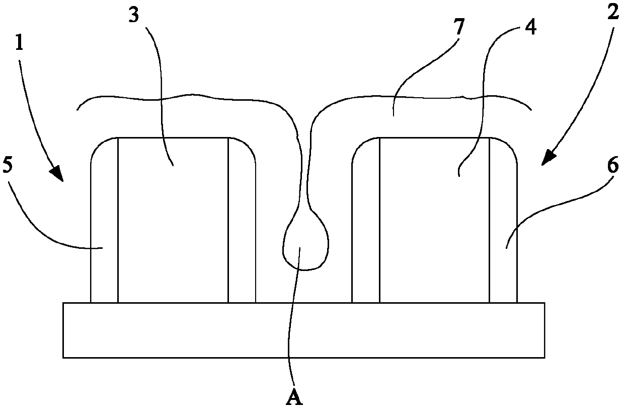
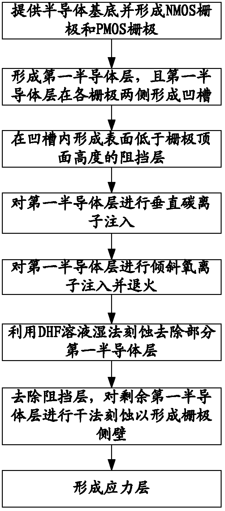
[0029] Such as figure 2 A method for forming a high-stress layer in a stress memory technology of the present invention shown, comprising steps:

[0030] providing a semiconductor substrate having PMOS and NMOS regions;

[0031] forming a PMOS gate and an NMOS gate on the PMOS region and the NMOS region, respectively;

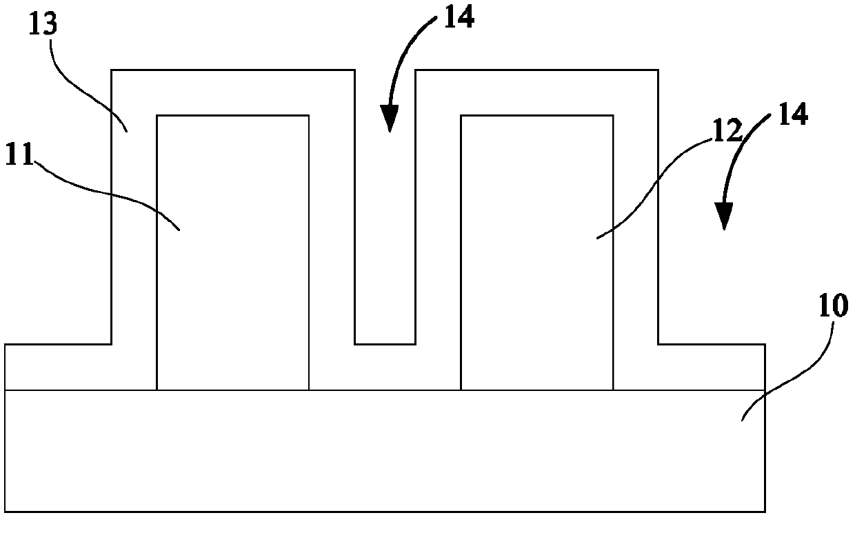
[0032] A first semiconductor layer is formed on the semiconductor substrate and the surface of the PMOS gate and the NMOS gate, and the first semiconductor layer forms grooves on both sides of each gate;

[0033] forming a barrier layer in the groove, the surface of...


PUM


Abstract

The invention provides a method for forming a stress layer in a stress memory technology. Grid electrode side walls are manufactured to cone-shaped side walls, and the horizontal width of each cone-shaped side wall gradually becomes larger in the direction perpendicular to the direction of a semiconductor base. The problems that a cavity exists in the stress layer between two grid structures due to too small intervals between the top ends of the two adjacent PMOS grid structure and NMOS grid structure, and then the device performance is affected are solved without affecting the follow-up ion implantation process.

Description

technical field [0001] The invention relates to the field of semiconductor manufacturing, in particular to a method for forming a stress layer in stress memory technology. Background technique [0002] In the semiconductor manufacturing process, especially when manufacturing CMOS (Complementary Metal-Oxide-Semiconductor, Complementary Metal-Oxide-Semiconductor) devices, it is known that in order to improve the performance of CMOS, stress technology is usually used to induce stress on the trench of the MOS transistor. road area. [0003] In the prior art, a typical process for providing stress to CMOS devices is called Stress Memorization Technique (SMT), and its general steps include: providing a semiconductor substrate with an NMOS region and a PMOS region; NMOS and PMOS gates and gate sidewall layers on both sides of the gate are formed on the NMOS and PMOS regions of the NMOS and PMOS regions; a stress layer formed by inherently strained materials is formed on the substr...

Claims


Application Information

Patent Timeline
IPC IPC(8): H01L21/8238
Inventor 隋运奇
Owner SEMICON MFG INT (SHANGHAI) CORP
Features
  • R&D
  • Intellectual Property
  • Life Sciences
  • Materials
  • Tech Scout
  • Unparalleled Data Quality
  • Higher Quality Content
  • 60% Fewer Hallucinations
Learn More