Metal oxide semiconductor electrical parameter testing device and method of manufacture

A technology of oxide semiconductors and electrical parameters, applied in semiconductor/solid-state device manufacturing, semiconductor devices, electric solid-state devices, etc., can solve problems such as threshold voltage drift, change of interface state, positive or negative charges cannot be released, etc., to achieve Threshold voltage change is small, and the effect of improving the interface state

Active Publication Date: 2013-10-30
FOUNDER MICROELECTRONICS INT
View PDF4 Cites 4 Cited by
  • Summary
  • Abstract
  • Description
  • Claims
  • Application Information

AI Technical Summary

Problems solved by technology

[0006] In metal-oxide-semiconductor devices with metal gates, if there is plasma damage, the introduced positive or n

Method used


Image

  • Metal oxide semiconductor electrical parameter testing device and method of manufacture
  • Metal oxide semiconductor electrical parameter testing device and method of manufacture
  • Metal oxide semiconductor electrical parameter testing device and method of manufacture

Examples


Embodiment Construction

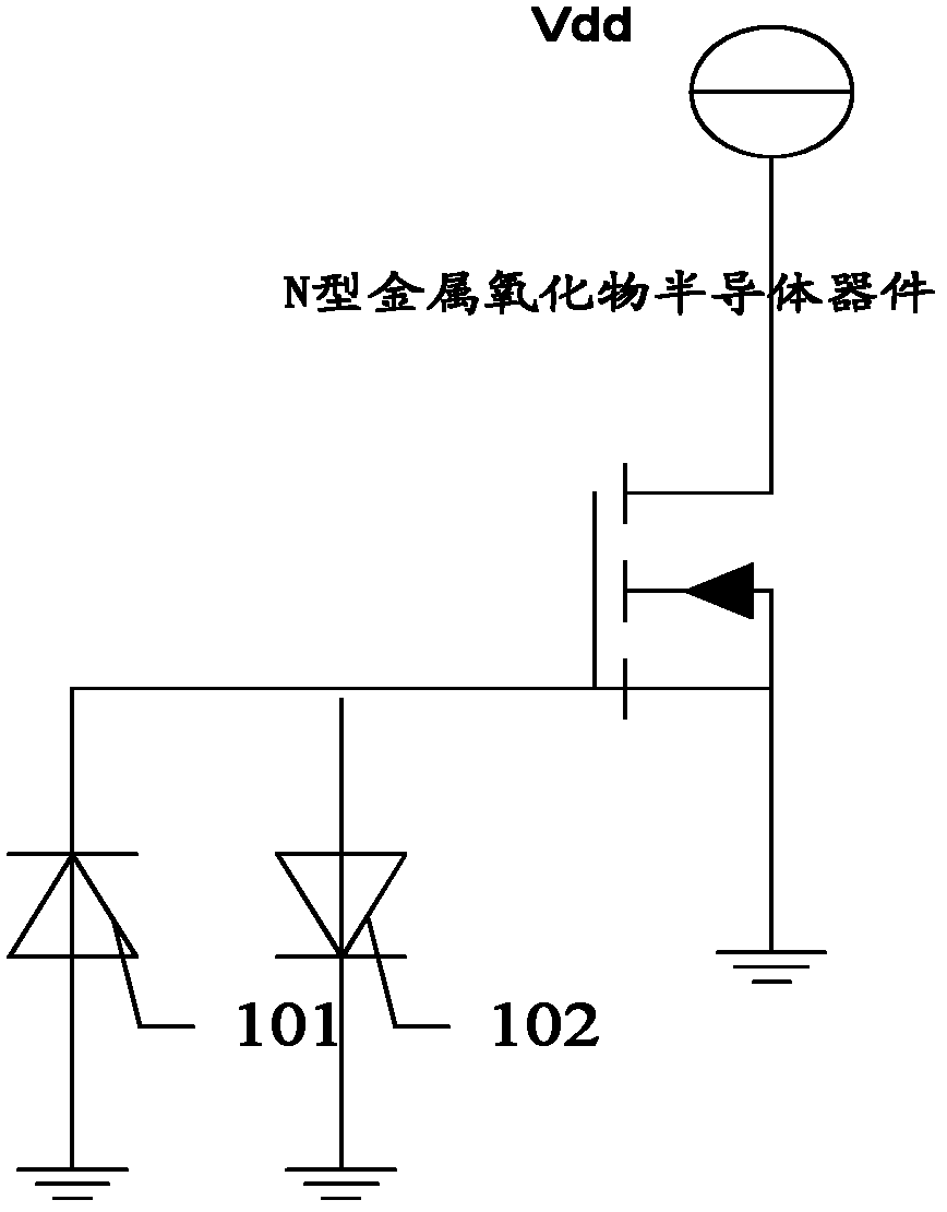
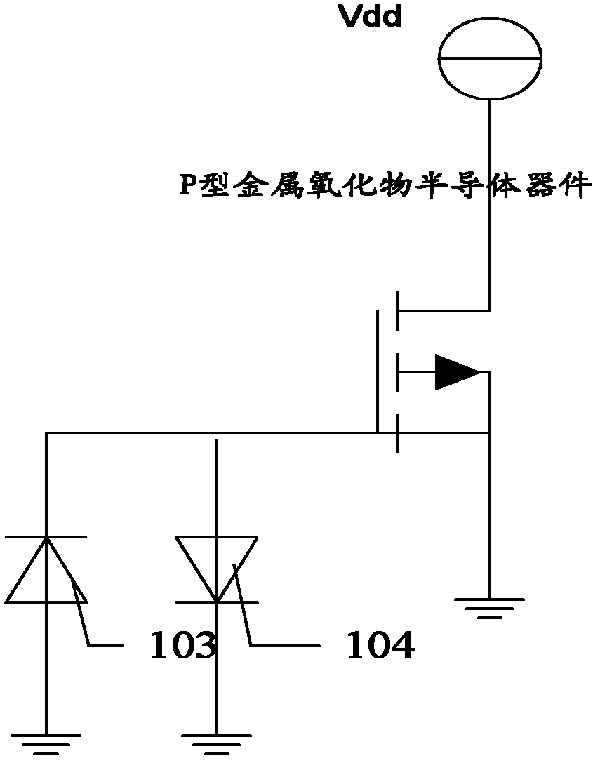
[0032] In the embodiment of the present invention, in the metal oxide semiconductor electrical parameter test device with metal as the gate, two parallel reverse diodes are connected through the gate to release the charge introduced by the gate due to plasma damage, thereby improving the interface state and making the threshold test The values ​​actually reflect the thresholds of the semiconductor devices in the circuit.

[0033] The schematic diagram of the composition of the N-type metal oxide semiconductor electrical parameter test device and the P-type metal oxide semiconductor electrical parameter test device in the first embodiment of the present invention is as follows Figure 1a and Figure 1b shown.

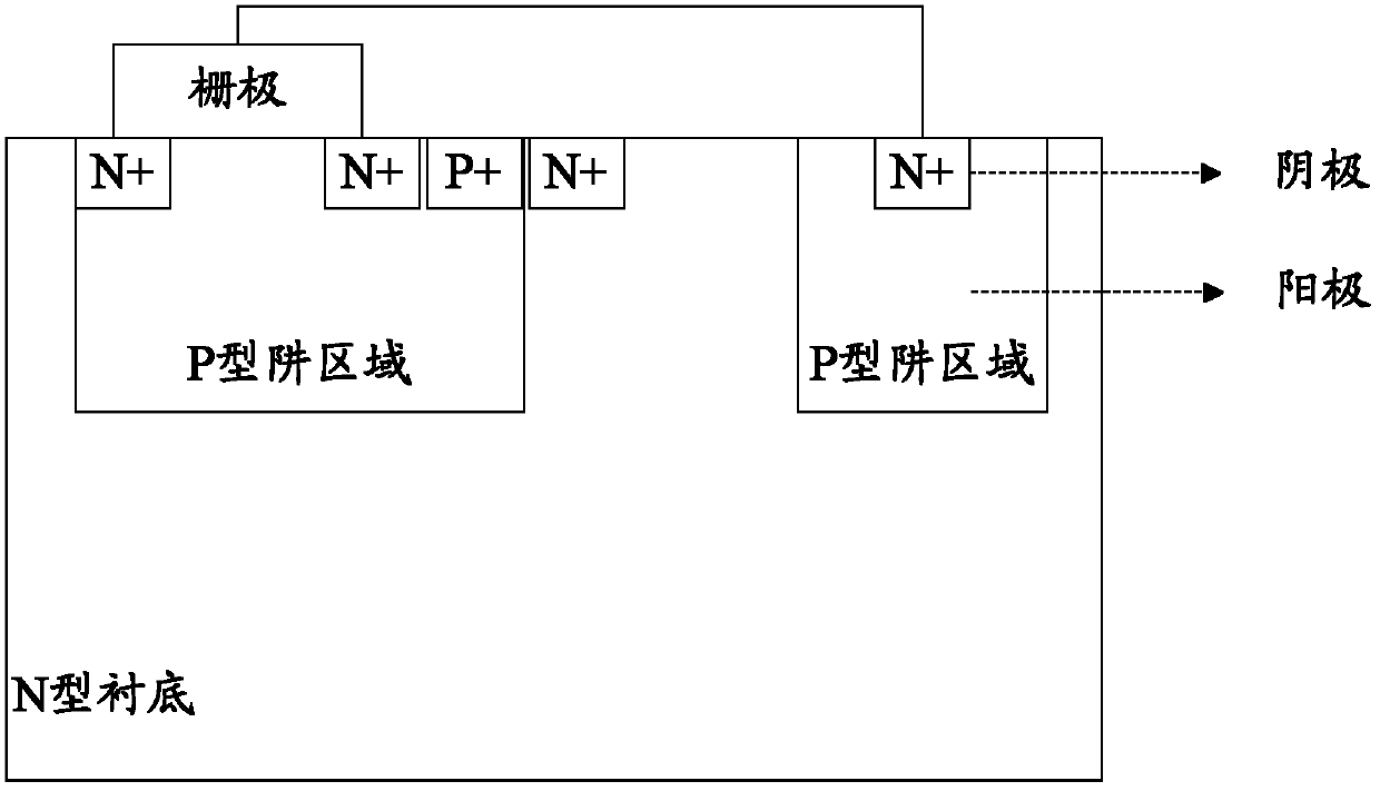
[0034] Figure 1a Among them, in the N-type metal oxide semiconductor electrical parameter test device with metal as the gate, the first PN structure formed by the first P-type well region of the N-type substrate and the first N+ region forms the first diode 101, so The...


PUM


Abstract

The invention discloses a metal oxide semiconductor electrical parameter testing device and a method of manufacture. A gate is a metal gate. A first P-type well region of an N-type substrate and a first N+ region form a first PN junction to constitute a first diode. A second P-type well region of the N-type substrate and a second N+ region form a second PN junction to constitute a second diode. The first diode is in anti-parallel connection with the second diode and is connected with the gate to form an N-type metal oxide semiconductor electrical parameter testing device. Or, the N-type substrate and the first P+ region form a third PN junction to constitute a third diode; the N-type substrate and the second P+ region form a fourth PN junction to constitute a fourth diode; and the third diode is in anti-parallel connection with the fourth diode and is connected with the gate to form a P-type metal oxide semiconductor electrical parameter testing device. According to the invention, positive charge or negative charge introduced due to plasma damage can be well discharged so as to enable small variation in threshold voltage.

Description

technical field [0001] The invention relates to the technical field of semiconductor manufacturing, in particular to a metal oxide semiconductor electrical parameter testing device and a manufacturing method. Background technique [0002] In modern semiconductor technology, especially in the manufacturing process of large-scale integrated circuits, in order to meet the special requirements of small-sized devices to avoid high-temperature thermal processes, more plasma processes are used in the production process. For example, active area etching, polysilicon gate etching, contact hole etching, metal wiring etching, passivation layer etching, etc. in the etching process; formation of metal wiring insulating layer, final passivation protection layer in thin film process formation etc. [0003] When using the plasma process, it will inevitably bring some problems, such as plasma damage, film stress change, etc., plasma damage will introduce positive or negative charges into th...

Claims


Application Information

Patent Timeline
IPC IPC(8): H01L27/06H01L21/82
Inventor 谭灿健
Owner FOUNDER MICROELECTRONICS INT
Why Eureka
Try Eureka