Light emitting diode encapsulation, PCB type radiating substrate used for light emitting diode encapsulation and manufacturing method of PCB type radiating substrate

A technology for heat-dissipating substrates and LED packaging, applied in printed circuit manufacturing, electrical components, circuits, etc., can solve unresolved problems, luminous efficiency, service life of heat-dissipating function, manufacturing cost, assembly yield, simplified manufacturing process, and difficulty in meeting requirements, etc. question

Inactive Publication Date: 2013-11-06
MAO BANG ELECTRONICS
View PDF26 Cites 21 Cited by
  • Summary
  • Abstract
  • Description
  • Claims
  • Application Information

AI Technical Summary

Problems solved by technology

Most of the above-mentioned existing technologies are aimed at the structure of an LED element or its packaging (package) structure, in terms of luminous efficiency, heat dissipation function, service life, manufacturing cost, assembly yield, simplification of the manufacturing process, and light decay. and deficiencies, and propose different technical means to solve these problems and deficiencies
However, as far as the applicant judges, the current existing technologies have not proposed an effective solution to the problem of how to achieve good heat dissipation without short-circuiting the circuit layer.
[0006] It can be seen from the above that the structure of the above-mentioned prior art is still difficult to meet the requirements of actual use, so there is still a need for further improvement in related fields such as LED packages or heat dissipation substrates used in LED packages or LED light emitting devices.

Method used


Image

  • Light emitting diode encapsulation, PCB type radiating substrate used for light emitting diode encapsulation and manufacturing method of PCB type radiating substrate
  • Light emitting diode encapsulation, PCB type radiating substrate used for light emitting diode encapsulation and manufacturing method of PCB type radiating substrate
  • Light emitting diode encapsulation, PCB type radiating substrate used for light emitting diode encapsulation and manufacturing method of PCB type radiating substrate

Examples


Embodiment Construction

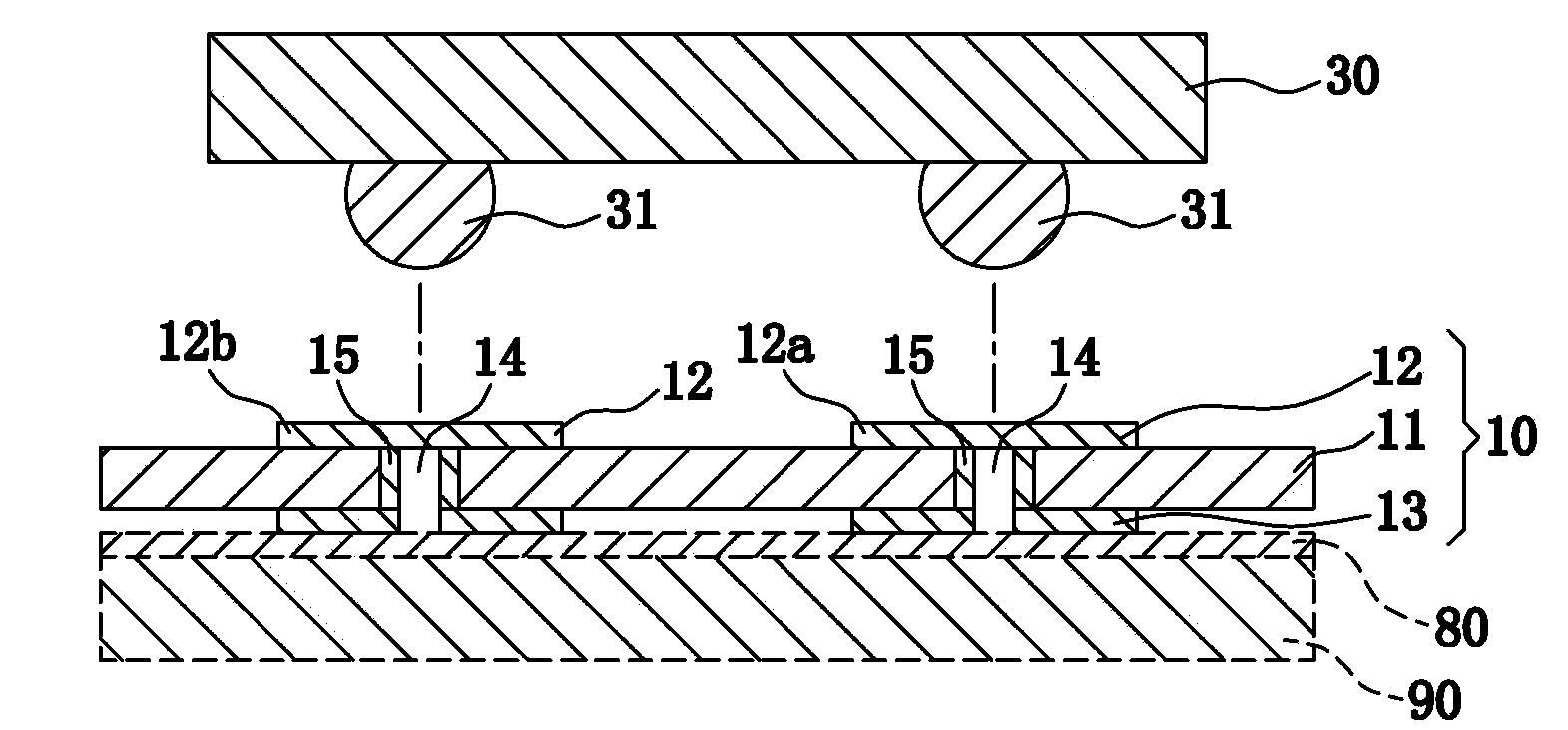
[0049] refer to Figure 3-10 As shown, they are schematic cross-sectional structural views of multiple embodiments of the PCB heat dissipation substrate and the formed LED package (LED package) of the present invention. The PCB type heat dissipation substrate 10 of the present invention is as image 3 As shown, it is made by using a printed circuit board (PCB, Printed Circuit Board) as Figures 11A-11E As shown (to be described later), it includes an insulating layer 11, a first circuit layer 12 and a second circuit layer 13; wherein the first circuit layer 12 is provided on the upper surface of the insulating layer 11 for light emitting The diode (LED) die 30 can be flip-chip (Flip Chip) such as Figure 4 , 6 As shown or the wire (Wire bond) method is as follows Figure 8 , 10 As shown, it is electrically connected on the PCB heat dissipation substrate 10 to form an LED package such as Figure 4 , 6 flip-chip LED packages as shown 40, 50 or as Figure 8 , 10 The wire...


PUM


Abstract

The invention discloses light emitting diode encapsulation, a PCB type radiating substrate used for the light emitting diode encapsulation and a manufacturing method of the PCB type radiating substrate. The PCB type radiating substrate is formed with a manufacturing method of a PCB and comprises an insulating layer, a first circuit layer and a second circuit layer, wherein the first circuit layer is arranged on the upper surface of the insulating layer and is used for being electrically connected with LED crystal particles through a flip chip or through a wire, the second circuit layer is arranged on the lower surface of the insulating layer, at least one heat conduction hole which penetrates between the upper surface of the insulating layer and the lower surface of the insulating layer is formed in the insulating layer, an electrocoppering layer is arranged on the inner wall of the heat conduction hole and is connected to the first circuit layer and the second circuit layer, and then the radiating coefficient is effectively increased. According to the light emitting diode encapsulation, the PCB type radiating substrate used for the light emitting diode encapsulation and the manufacturing method of the PCB type radiating substrate, the heat conduction hole can be filled with heat conduction materials to further increase the radiating coefficient; the LED crystal particles can be electrically connected to the PCB type radiating substrate through the flip chip or through the wire according to manufacturing requirements to achieve the light emitting diode encapsulation; a bonding layer is arranged outside the second circuit layer to enable the LED encapsulation to be connected to and fixedly arranged on a radiating bracket of an LED light-emitting device to serve as a light source of the LED light emitting device.

Description

technical field [0001] The present invention relates to a light-emitting diode package (LED package) and the used PCB heat dissipation substrate and its manufacturing method, especially to a printed circuit board (PCB) manufacturing method to form a PCB heat dissipation substrate for an LED crystal grain It is electrically connected to the PCB type heat dissipation substrate in the form of flip chip or wire to complete an LED package, so as to achieve good heat dissipation effect. Background technique [0002] Generally speaking, an LED chip can be selected as flip chip (Flip Chip) or wire bond (Wire bond) according to the needs of the production process, but not limited, to be electrically connected to a heat dissipation substrate with a circuit layer to complete. An LED package (LED package), which is then connected and fixed on a heat sink (or heat sink or lamp holder) of a light-emitting device to become the light source of the light-emitting device, thus completing an L...

Claims


Application Information

Patent Timeline
Patent Type & Authority Applications(China)
IPC IPC(8): H01L33/48H01L33/64H01L33/00H05K1/02H05K3/00
CPCH01L2224/16H01L2224/16225H01L2224/32225H01L2224/48091H01L2224/48227H01L2224/73265H01L2224/92247H01L2924/00014H01L2924/00
Inventor 赖东升宋大仑
Owner MAO BANG ELECTRONICS
Why Eureka
Try Eureka