Supercharge Your Innovation With Domain-Expert AI Agents!

Line pattern manufacturing method

A technology of circuit patterns and manufacturing methods, which is applied in the direction of removing conductive materials by chemical/electrolytic methods, containing printed electrical components, and secondary processing of printed circuits.

Inactive Publication Date: 2013-11-06
LEADING TECH COMM
View PDF5 Cites 3 Cited by
  • Summary
  • Abstract
  • Description
  • Claims
  • Application Information

AI Technical Summary

Problems solved by technology

The possible problems caused by the above-mentioned laser direct forming antenna structure are worthy of further improvement in the manufacture of antennas or other related conductive circuits in this field

Method used


Image

  • Line pattern manufacturing method
  • Line pattern manufacturing method
  • Line pattern manufacturing method

Examples


Embodiment Construction

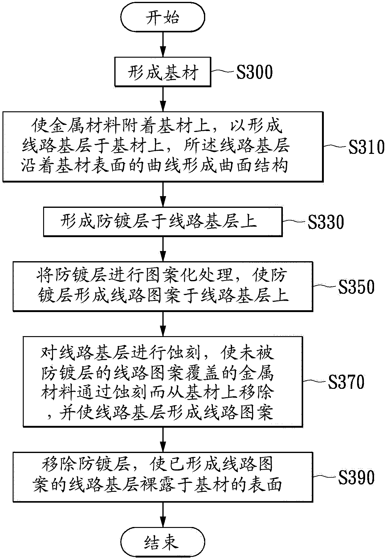
[0026] [Example of Manufacturing Method of Circuit Pattern]

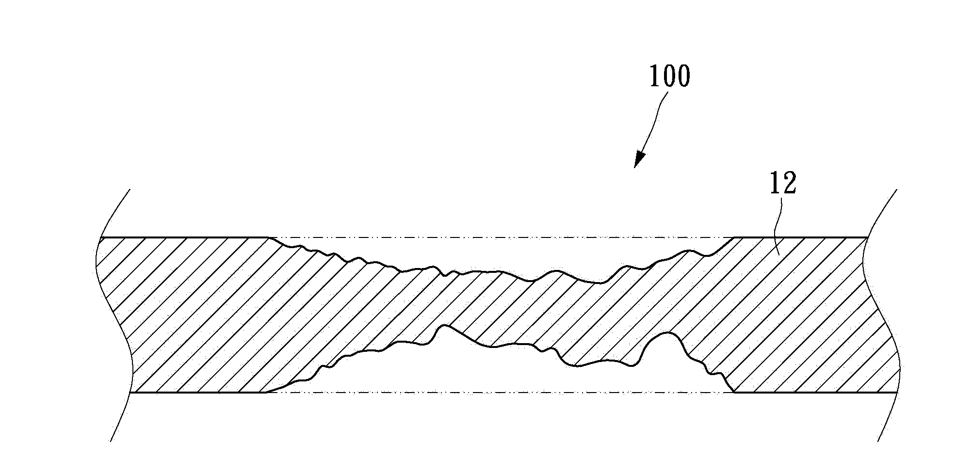
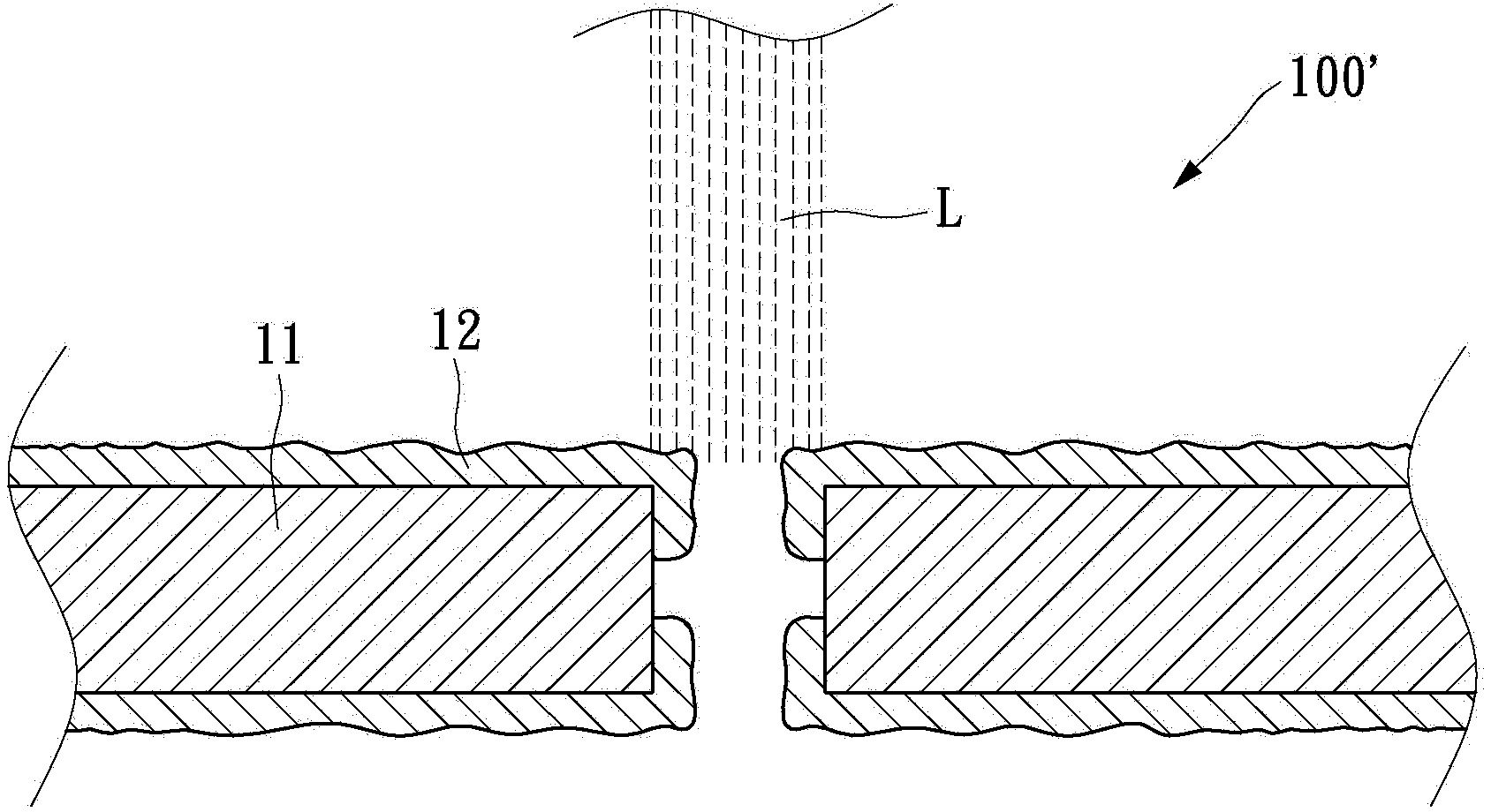
[0027] The manufacturing method of the circuit pattern in the embodiment of the present invention can form a three-dimensional patterned or curved antenna structure, or a circuit pattern for other purposes on a commonly used substrate. The manufacturing method of the circuit pattern in the embodiment of the present invention is described by taking the manufacture of the antenna structure as an example, but the present invention is not limited to the manufacture of the antenna structure. In this embodiment, the base material is, for example, a case of a smart phone, and the case of a smart phone is usually made of plastic or glass. However, the present invention does not therefore limit the type of substrate. In order to provide sufficient bonding force of the antenna structure on the base material, this embodiment is described by taking the manufacture of the antenna structure on the casing as an example.

[0028]...


PUM

PropertyMeasurementUnit
Sizeaaaaaaaaaa

Abstract

The invention provides a line pattern manufacturing method. The method includes the following steps of firstly, forming a base material, secondly, attaching a metal material to the base material so as to form a line base layer on the base material, wherein the line base layer forms a curved surface structure along a curved line of the surface of the base material, thirdly, forming an anti-plating layer on the line base layer, fourthly, etching the line base layer, removing the metal material which is not covered by a line pattern of the anti-plating layer from the base material in an etching mode and enabling the line base layer to form a line pattern, and finally, removing the anti-plating layer so as to enable the line base layer with the line pattern to be exposed out of the surface of the base material. Therefore, manufacturing cost of the line patterns can be reduced, and manufacturing quality of the line patterns are improved.

Description

technical field [0001] The invention relates to a circuit pattern, in particular to a method for manufacturing the circuit pattern. Background technique [0002] figure 1 and figure 2 is a schematic diagram of a conventional antenna structure 100, 100'. like figure 1 It shows a laser active layer 12 formed on a substrate 11 by using a laser direct structuring (Laser Direct Structuring, LDS) process. The substrate 11 may be a casing of a mobile device (eg, a smart phone). Since some areas are not fully activated by the laser, unevenness occurs (the dotted line is the ideal line width), such as jump plating, which may affect the overall effect of the antenna structure. another example figure 2 As shown, when some substrates 11 with through holes are activated with laser beam L, due to the influence of factors such as the size and shape of the through holes, the angle of the laser, some areas in the hole walls may not be fully activated by the laser, and then The upper...

Claims


Application Information

Patent Timeline
IPC IPC(8): H05K3/06H05K3/38H05K1/16
Inventor 黄兴亚
Owner LEADING TECH COMM
Features
  • R&D
  • Intellectual Property
  • Life Sciences
  • Materials
  • Tech Scout
  • Unparalleled Data Quality
  • Higher Quality Content
  • 60% Fewer Hallucinations
Learn More