Method for manufacturing thin silicon wafer

A silicon wafer and silicon nitride technology, which is applied in semiconductor/solid-state device manufacturing, electrical components, circuits, etc., can solve the problems that silicon wafers cannot be ground to a very thin size, and the fragmentation rate is high, so as to reduce production costs and Large warpage and reduced equipment cost

Active Publication Date: 2013-11-13
SHANGHAI HUAHONG GRACE SEMICON MFG CORP
View PDF4 Cites 5 Cited by
  • Summary
  • Abstract
  • Description
  • Claims
  • Application Information

AI Technical Summary

Problems solved by technology

In the silicon wafer thinning process, it is generally not possible to grind the silicon wafer to a very thin size, because if the silicon wafer is directly ground to the thickness required for the chip package, due to the existence of the mechanical damage layer, in the transportation and subsequent processes very high fragmentation rate

Method used


Image

  • Method for manufacturing thin silicon wafer
  • Method for manufacturing thin silicon wafer

Examples


Embodiment Construction

[0024] In order to have a more specific understanding of the technical content, characteristics and effects of the present invention, now in conjunction with the illustrated embodiment, the details are as follows:

[0025] The preparation method of the thin silicon wafer of the present embodiment comprises the following process steps:

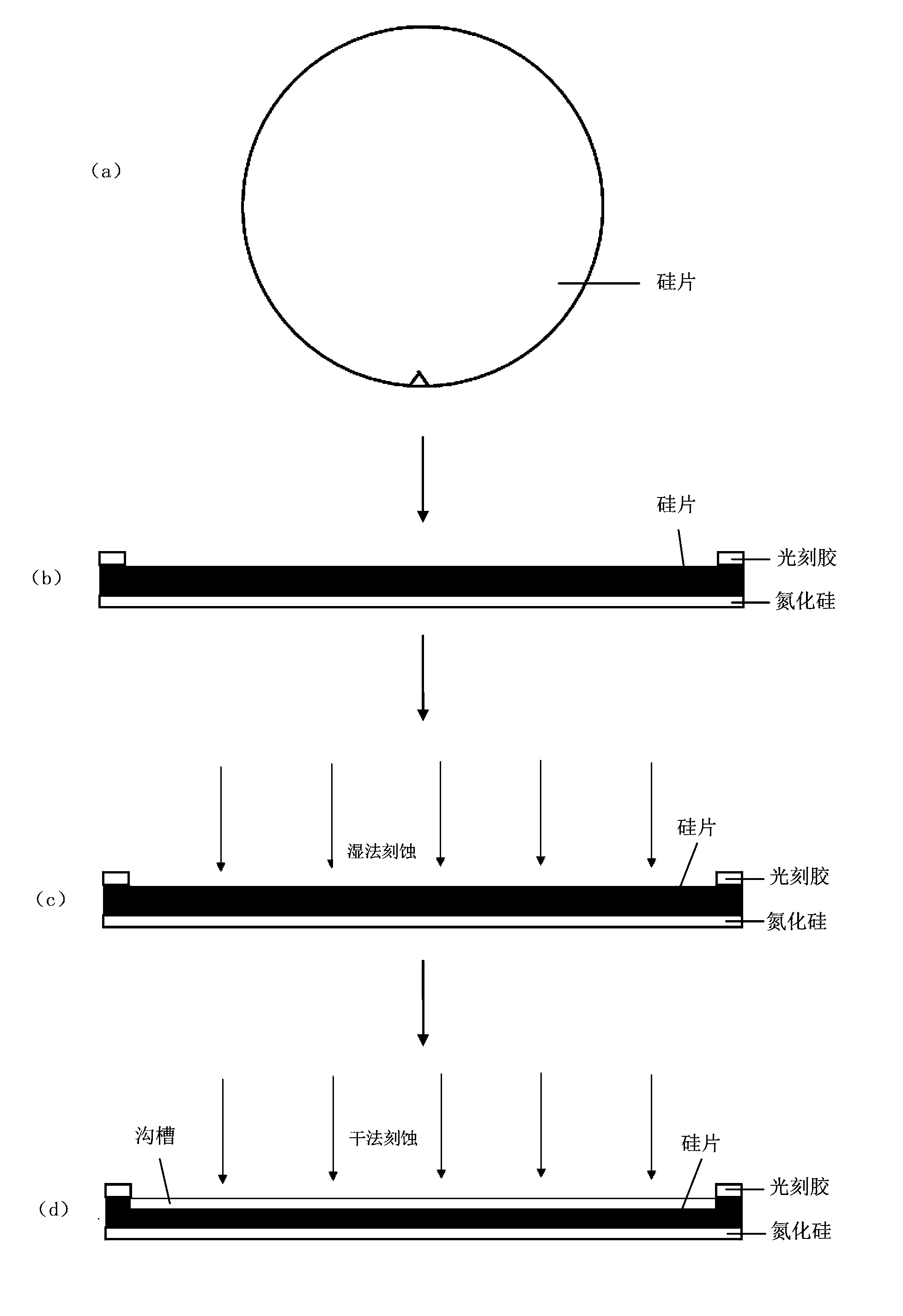
[0026] Step 1, grow a layer of silicon nitride on the front surface of a silicon wafer with a thickness of 725 μm and a diameter of 200 mm, such as figure 1 (a) shown.

[0027] For the type of silicon wafer, in addition to the above-mentioned sizes, existing industrial standard silicon wafers of various sizes can also be used, such as 4 inches, 6 inches, 8 inches, 12 inches, etc.

[0028] Silicon nitride is deposited by LPCVD (low pressure chemical vapor deposition) process, and its thickness depends on the thickness of the oxide to be etched later.

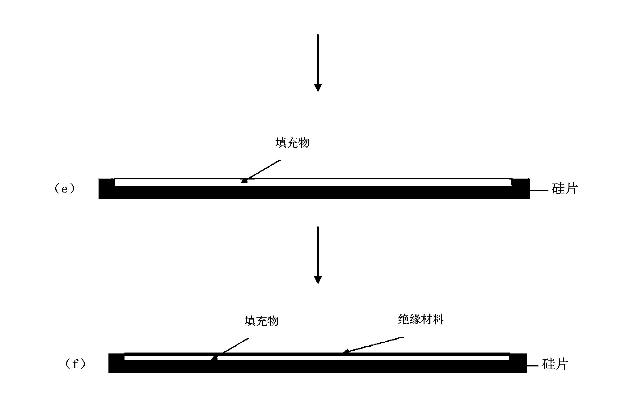
[0029] Step 2, coat a layer of negative photoresist on the back of the silicon wafer, then e...


PUM

PropertyMeasurementUnit
Thicknessaaaaaaaaaa
Diameteraaaaaaaaaa
Widthaaaaaaaaaa

Abstract

The invention discloses a method for manufacturing a thin silicon wafer. The method includes the following steps: (1) growing silicon nitride or silicon oxynitride on a silicon wafer with the traditional thickness, (2) coating the back face of the silicon wafer with photoresist, exposing and developing the periphery of the silicon wafer, and enabling the photoresist to be only remained on the periphery of the back face of the silicon wafer, (3) etching a trench in the position, where the photoresist is not located, of the back face of the silicon wafer, (4) filling the trench with electric-conduction heat-conduction materials, and (5) sealing the electric-conduction heat-conduction materials with a layer of insulation materials again, and enabling the following processes to be carried out according to the traditional processes to complete the manufacturing of the thin silicon wafer. According to the method for manufacturing the thin silicon wafer, the trench is formed in the back face of the silicon wafer and filled with the metal materials or the insulation materials, therefore, the large warping degree problem caused by the fact that the silicon wafer is thinned is effectively solved, and the thickness of the silicon wafer can be reduced to be 20mm to 500mm. In addition, the method for manufacturing the thin silicon wafer is based on the existing processes, existing production lines can be sufficiently used, therefore, the device cost is reduced, and the production cost is reduced.

Description

technical field [0001] The invention relates to the field of semiconductor integrated circuit manufacturing, in particular to a method for preparing a thin silicon wafer. Background technique [0002] The effective thickness of the circuit layer on the silicon wafer is generally 5-10 mm. In order to ensure its function, a certain supporting thickness is necessary. Therefore, the thickness limit of the circuit layer on the silicon wafer is 20-30 mm. The 20-30mm only accounts for a small part of the total thickness of the silicon wafer, and about 90% of the total thickness is the substrate material, which is to ensure that the silicon wafer has sufficient strength during manufacturing, testing and transportation. Therefore, after the circuit layer is fabricated, it is necessary to perform backside thinning on the silicon wafer to achieve the desired thickness, and then perform dicing on the silicon wafer to form thinned dies one by one. chip. [0003] The thinned chip has th...

Claims


Application Information

Patent Timeline
IPC IPC(8): H01L21/02
Inventor 孟鸿林郭晓波刘尧
Owner SHANGHAI HUAHONG GRACE SEMICON MFG CORP
Why Eureka
Try Eureka