Method for processing PCB with step groove

A PCB board and processing method technology, applied in the field of PCB board manufacturing, can solve problems such as retention in holes, PCB board damage, delamination explosion, etc., to achieve the effect of ensuring flatness and avoiding circuit short circuit or open circuit of PCB board

Active Publication Date: 2013-11-13
SHENNAN CIRCUITS
View PDF4 Cites 28 Cited by
  • Summary
  • Abstract
  • Description
  • Claims
  • Application Information

AI Technical Summary

Problems solved by technology

Please refer to the invention patent with the Chinese patent application number 200910307869.X, which mainly adopts the method of secondary pressing to produce a PCB board with stepped grooves. Before electroplating, the holes will be filled with insulating resin. Although this method can Avoid the phenomenon that the electroplating solution enters the multilayer printed circuit board from the hole at the bottom of the circuit board to cause corrosion of the hole wall and/or the inner circuit of the printed circuit board, but the insulating resin filled in can only stay in the hole, if

Method used


Image

  • Method for processing PCB with step groove
  • Method for processing PCB with step groove

Examples


Embodiment Construction

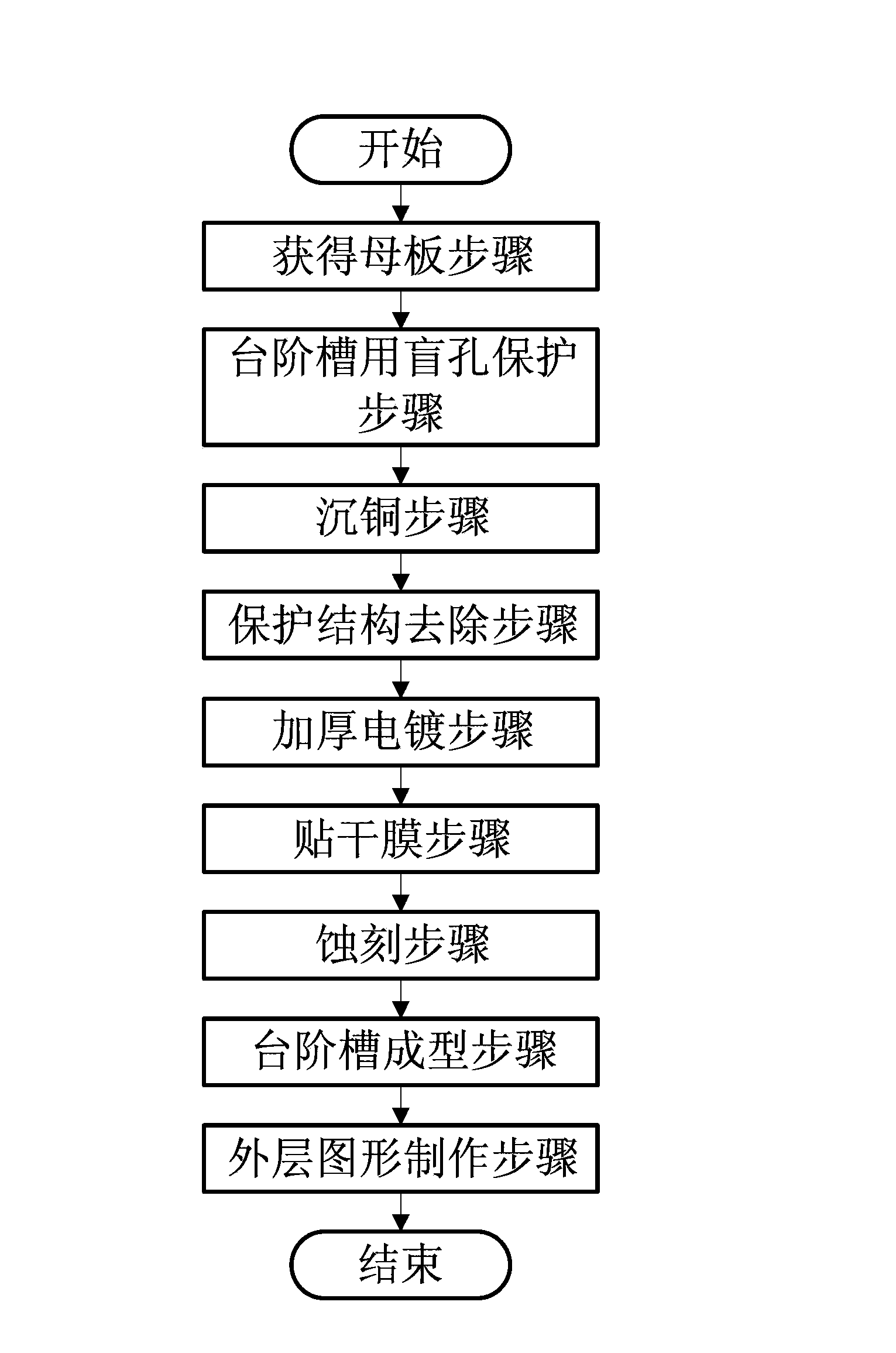
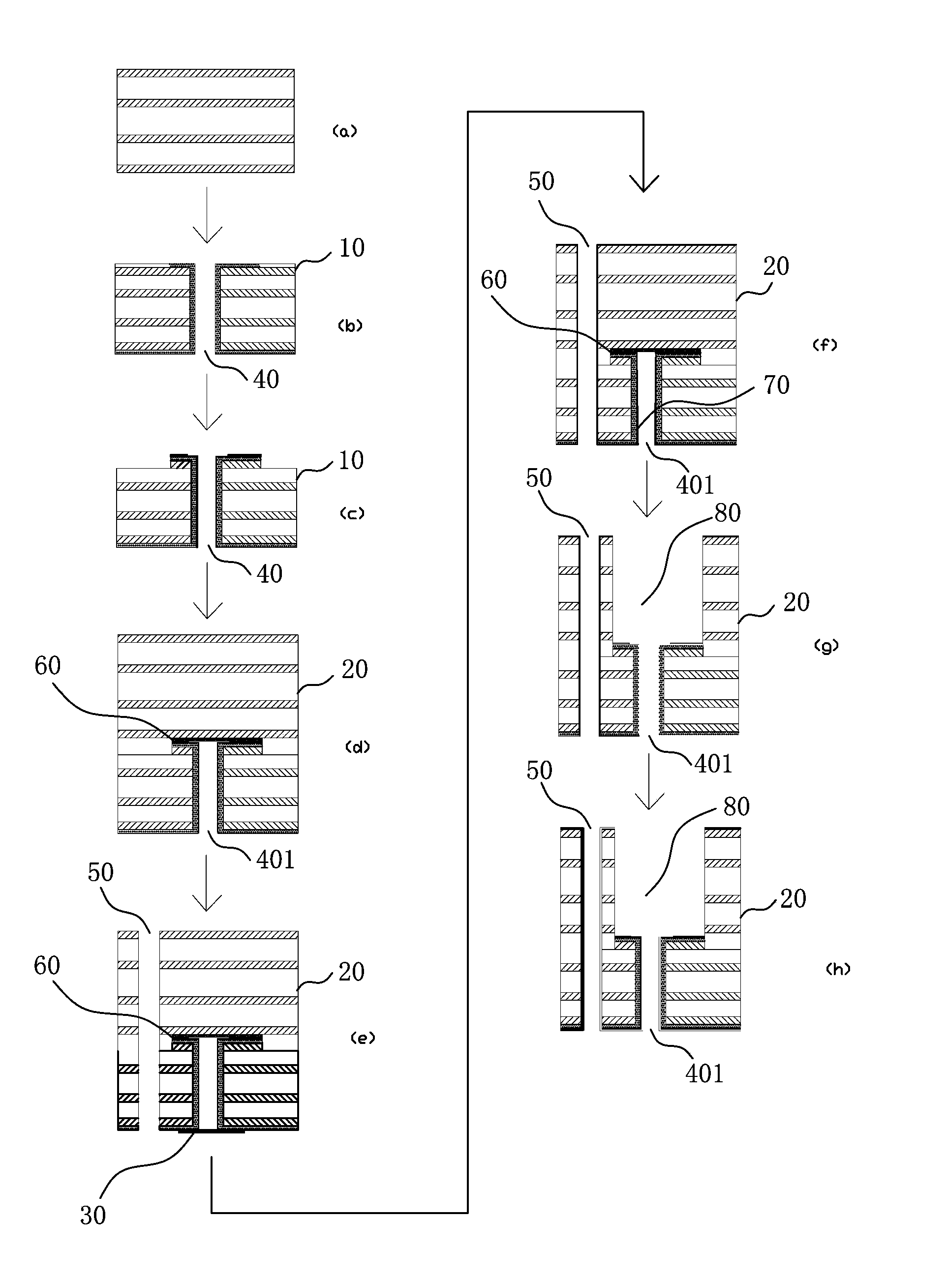
[0016] The processing method of the PCB board with stepped grooves in the embodiment of the present invention is mainly to pre-coat the bottom edge and hole wall of the blind hole with the stepped groove with a resist layer, and set the protective structure on the stepped groove before the mother board sinks copper. Use the hole of the blind hole, remove the copper after sinking, effectively prevent the highly corrosive copper sinking solution from penetrating into the blind hole for the step groove and the graphic area at the bottom of the step groove and ensure the surface of the circuit board in the subsequent electroplating process Uniformity of copper thickness (the step of sinking copper usually only forms a copper layer with a thickness of a few microns, which does not affect the consistency of the thickness of the copper layer after subsequent electroplating, so it does not affect the transmission of signals after the formation of subsequent lines), and at the same time,...


PUM


Abstract

The invention discloses a method for processing a PCB with a step groove. The method for processing the PCB with the step groove comprises the step of obtaining of a parent plate, the step of protection of a blind hole for the step groove, the step of copper electroless plating, the step of removal of a protective structure, the step of plating thickening, the step of pasting of dry film, the step of etching and the step of forming of the step groove. Due to the fact that the technological means that a corrosion resistant layer coats the edge of the bottom and the hole wall of the blind hole for the step groove in advance, the protective structure is arranged in a hole opening of the blind hole for the step groove before the copper electroless plating is carried out on the parent plate, the protective structure is removed after the copper electroless plating is finished, etching is carried out on a thickened copper plating layer in the blind hole for the step groove to completely remove the thickened copper plating layer through corrosion resistance of the corrosion resistant layer to alkaline etching liquid, a taper hole is prevented from forming, and finally a compression joint hole applicable to compression joint of an electrical apparatus element is manufactured in the bottom of the step groove is used, damage caused by copper electroless plating chemical liquid is effectively prevented, and the compression joint hole which is applicable to compression joint of the electrical apparatus element is manufactured in the bottom of the step groove. Meanwhile, a graph which is used for circuit connection is arranged at the bottom of the step groove, and the flatness of the plate surface of the parent plate is ensured due to the fact that the protective structure is timely removed.

Description

technical field [0001] The invention relates to the field of PCB board manufacturing, in particular to a method for processing a PCB board with stepped grooves. Background technique [0002] Generally, stepped grooves are provided on the PCB board to accommodate electrical components, so as to prevent the electrical components from protruding out of the circuit board and occupying the external space. Please refer to the invention patent with the Chinese patent application number 200910307869.X, which mainly adopts the method of secondary pressing to produce a PCB board with stepped grooves. Before electroplating, the holes will be filled with insulating resin. Although this method can Avoid the phenomenon that the electroplating solution enters the multilayer printed circuit board from the hole at the bottom of the circuit board to cause corrosion of the hole wall and / or the inner circuit of the printed circuit board, but the insulating resin filled in can only stay in the h...

Claims


Application Information

Patent Timeline
IPC IPC(8): H05K3/00H05K3/40
Inventor 钱文鲲陈于春许瑛沙雷
Owner SHENNAN CIRCUITS
Why Eureka
Try Eureka