Method for etching silicide-blocked oxide layer

A technology for blocking oxides and silicides, used in electrical components, semiconductor/solid-state device manufacturing, circuits, etc., can solve the problem that the thickness and uniformity of the remaining silicide blocking oxide layer cannot be well controlled Etch speed and etch uniformity

Inactive Publication Date: 2013-12-11
SHANGHAI HUAHONG GRACE SEMICON MFG CORP
View PDF3 Cites 2 Cited by
  • Summary
  • Abstract
  • Description
  • Claims
  • Application Information

AI Technical Summary

Problems solved by technology

[0007] However, in the prior art, when dry etching is used to partially etch the silicide blocking oxide layer, for the silicide blocking oxide layer with a total thickness of 300-400 Å, it is often not well controlled to silicidate. The etch speed and etch

Method used


Image

  • Method for etching silicide-blocked oxide layer

Examples


Embodiment Construction

[0023] In order to make the content of the present invention clearer and easier to understand, the content of the present invention will be described in detail below in conjunction with specific embodiments and accompanying drawings.

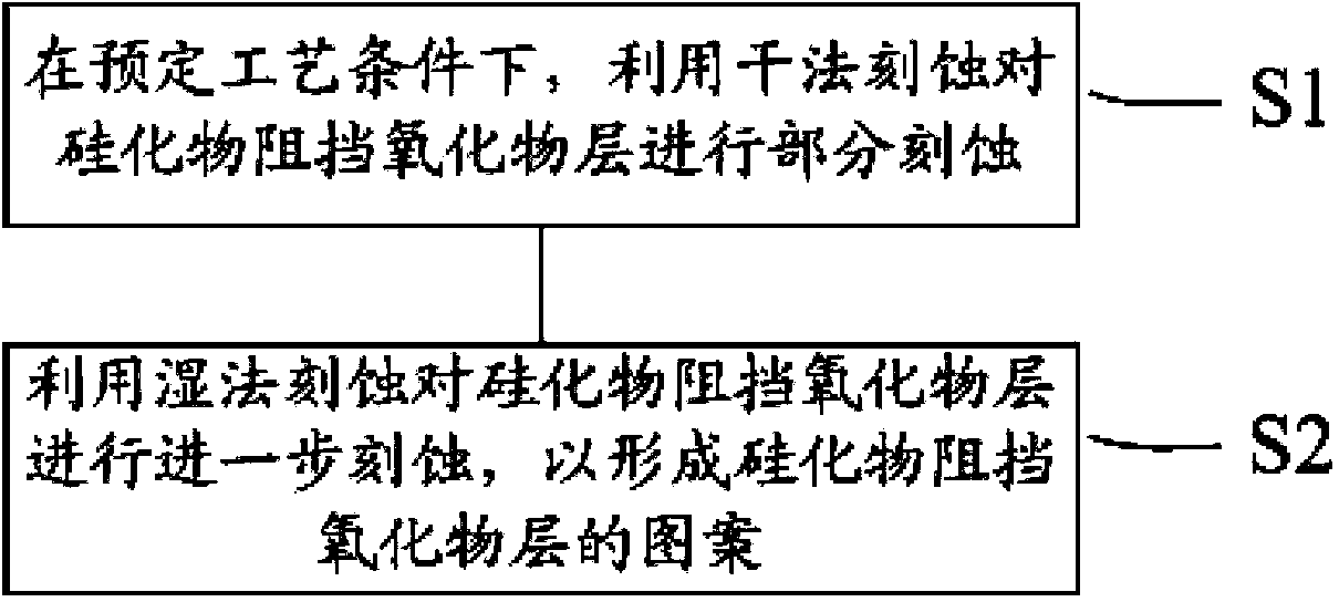
[0024] figure 1 A flow chart of a method for etching a silicide blocking oxide layer according to a preferred embodiment of the present invention is schematically shown.

[0025] The method is particularly suitable for etching silicide blocking oxide layers with a total thickness of 300-400A. Therefore, in this embodiment, the total thickness of the selective silicide blocking oxide layer is 300-400 Å.

[0026] Specifically, as figure 1 As shown, the etching method for the silicide blocking oxide layer according to the preferred embodiment of the present invention includes:

[0027] The first etching step S1: performing partial etching on the silicide blocking oxide layer by dry etching under predetermined process conditions;

[0028] Prefer...


PUM


Abstract

The invention provides a method for etching a silicide-blocked oxide layer. The method includes the steps that in predetermined technological conditions, partial etching is performed on the silicide-blocked oxide layer through dry etching; further etching is performed on the silicide-blocked oxide layer through wet etching so as to form patterns of the silicide-blocked oxide layer. The predetermined technological conditions are that etching power is 150W-250W, pressure is 50mT-100mT, and etching time is not less than 10 seconds.

Description

technical field [0001] The invention relates to the field of semiconductor manufacturing, and more specifically, the invention relates to an etching method for a silicide blocking oxide layer. Background technique [0002] The salicide block layer (SAB) is used to protect the surface of the silicon wafer. Under its protection, the silicon wafer does not form undesired metal silicides with other metals such as Ti and Co. [0003] In some processes, an oxide layer is used as a silicide barrier. [0004] The oxide layer that acts as a silicide barrier layer (referred to herein as the "silicide barrier oxide layer") needs to be etched to form the silicide barrier oxide layer pattern; thus, the silicide barrier oxide remaining after etching No metal silicide will be formed on the surface of the silicon wafer below the layer; however, metal silicide will be formed on the surface of the silicon wafer where the silicide blocking oxide layer is removed after etching. [0005] Initi...

Claims


Application Information

Patent Timeline
IPC IPC(8): H01L21/311H01L21/02
Inventor 肖培
Owner SHANGHAI HUAHONG GRACE SEMICON MFG CORP
Why Eureka
Try Eureka