Eureka AIR delivers breakthrough ideas for toughest innovation challenges, trusted by R&D personnel around the world.

A Microstructure Plasma Device Based on Printed Circuit Board Technology

A technology for printed circuit boards and ion devices, which is applied in the directions of plasma and electrical components, and achieves the effects of less process links, simple and feasible process, and extremely easy production and production.

Inactive Publication Date: 2016-04-27
HENAN POLYTECHNIC UNIV
View PDF5 Cites 0 Cited by
  • Summary
  • Abstract
  • Description
  • Claims
  • Application Information

AI Technical Summary

Problems solved by technology

However, the disadvantage of making microstructure devices in the past is that high-precision processing instruments and advanced technology are required for support.

Method used


Image

  • A Microstructure Plasma Device Based on Printed Circuit Board Technology
  • A Microstructure Plasma Device Based on Printed Circuit Board Technology
  • A Microstructure Plasma Device Based on Printed Circuit Board Technology

Examples


Embodiment Construction

[0022] The present invention will be described in further detail below.

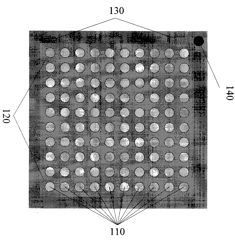
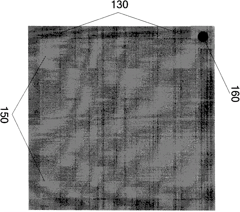
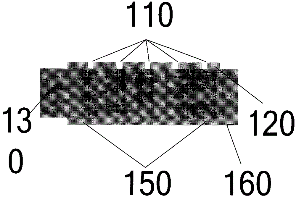
[0023] The device microcavity is composed of an upper electrode, an intermediate dielectric layer and a lower electrode, and each unit of the device is driven by the upper and lower electrodes. Take the insulating dielectric epoxy resin material as the base, make two layers of copper foil on the upper and lower surfaces of the base, leaving a certain safe distance between the edge of the copper foil and the edge of the base. Cylindrical microcavity semi-through holes (just pass through the upper electrode but not the middle dielectric layer and the lower electrode) units are arranged in an array, and the distance between rows in the array is not less than the distance between columns. The upper and lower layers of copper foil separated by the bottom plate are used as the upper and lower electrodes, and the two electrodes are respectively led out of the connection terminals, thus obtaining a coplanar microst...


PUM

PropertyMeasurementUnit
thicknessaaaaaaaaaa
thicknessaaaaaaaaaa

Abstract

Disclosed is a microstructural plasma device based on a printed circuit board process. A microcavity of the device is composed of an upper electrode, a middle medium layer and a lower electrode. Each unit of the device is driven by the upper electrode and the lower electrode. A substrate is made of insulating medium epoxy resin materials. Two layers of copper foil are manufactured on the upper surface and the lower surface of the substrate. Certain safe distances are reserved between the edges of the layers of copper foil and the edge of the substrate. The cylindrical microcavity semi-through hole units are arranged in an array mode. Microcavity semi-through holes just penetrate through the upper electrode and do not penetrate through the middle medium layer and the lower electrode. In the array, the distances between rows are not smaller than those between columns. The two layers of copper foil which are separated by the substrate are used as the upper electrode and the lower electrode, the two electrodes are respectively led out of amphenol connectors, and the coplanar-type microstructural plasma device based on the printed circuit board process is obtained.

Description

Technical field [0001] The invention relates to a microstructure plasma device based on a printed circuit board process. Background technique [0002] In recent years, as a new type of low-temperature plasma source, micro-discharge plasma has become a hot research topic in the field of low-temperature plasma due to its wide application prospects and the great possibility of opening up many emerging low-temperature plasma basic research fields. one. [0003] The so-called micro-structured discharge plasma refers to the plasma whose spatial characteristic dimension is restricted to the order of sub-millimeter to micrometer. It is usually produced by the miniaturization of conventional plasma devices. Although it is developed from conventional plasma, the size of the discharge is reduced to the order of millimeters or even lower, so that the micro-discharge plasma can usually operate under atmospheric pressure. Compared with conventional plasma, there have been some new changes, su...

Claims


Application Information

Patent Timeline
Patent Type & Authority Patents(China)
IPC IPC(8): H05H1/24
Inventor 孙岩洲赵来军张展韦延方卫林林巩银苗
Owner HENAN POLYTECHNIC UNIV
Why Eureka
Eureka Blog
Learn More