
Eureka
For R&D, Eureka makes reading and utilizing patents & technical documents easy.
Eureka AIR
Designed for self-driven R&D workflows. Generate viable solutions, solve complex R&D challenges, empower your innovation with AI.

Eureka Materials
Designed for material experts only. Revolutionize your material R&D, from search, analyze, to developing new materials.

TechResearch
Generate reliable direction feasibility study reports for your R&D in just a few steps.

TechSeek
Discover and master advanced knowledge NOW. Basics, ideas, possibilities, all at once.

TechMind
As an expert in R&D Theories, TechMind can generates customized viable solutions instantly.

TechRisk
Analyze your overall solution with one click, know your potential R&D risks in advance.

TechMonitor
Get weekly tech updates, stay abreast of the latest tech innovations and key insights.
Semiconductor structure with improved channel stack and method for fabrication thereof
A semiconductor, stacking technology used in semiconductor/solid-state device manufacturing, semiconductor devices, electro-solid devices, etc., to solve problems such as diffusion of dopant materials, degradation of performance, and interference with reliable transistor operation
- Summary
- Abstract
- Description
- Claims
- Application Information
AI Technical Summary
Problems solved by technology
Method used
Image

Examples
Embodiment Construction
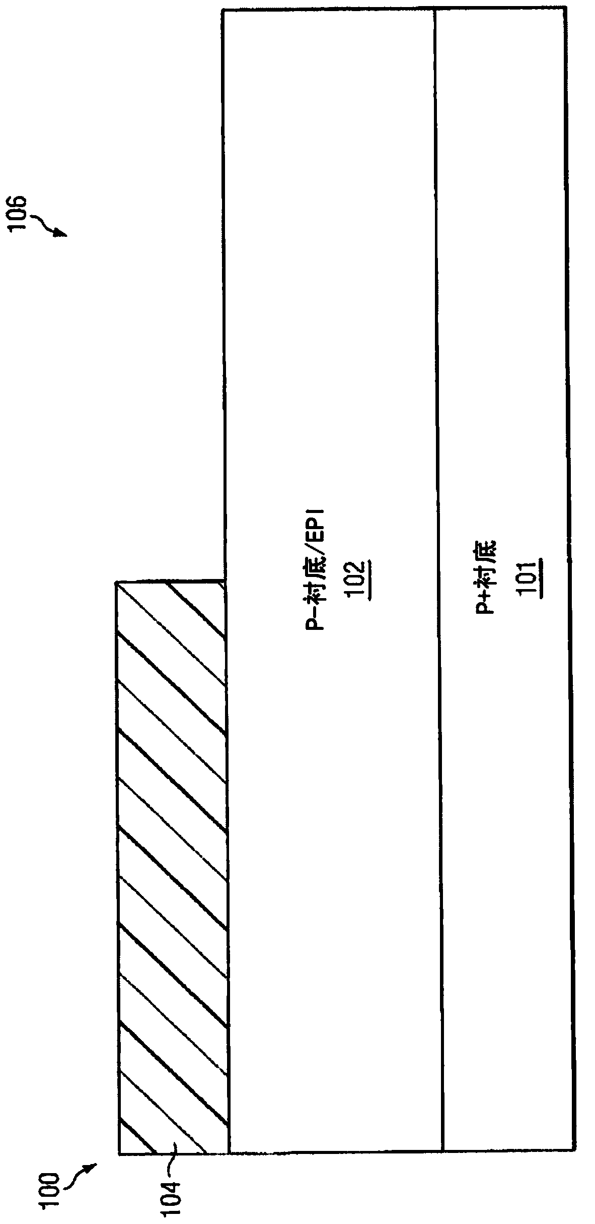
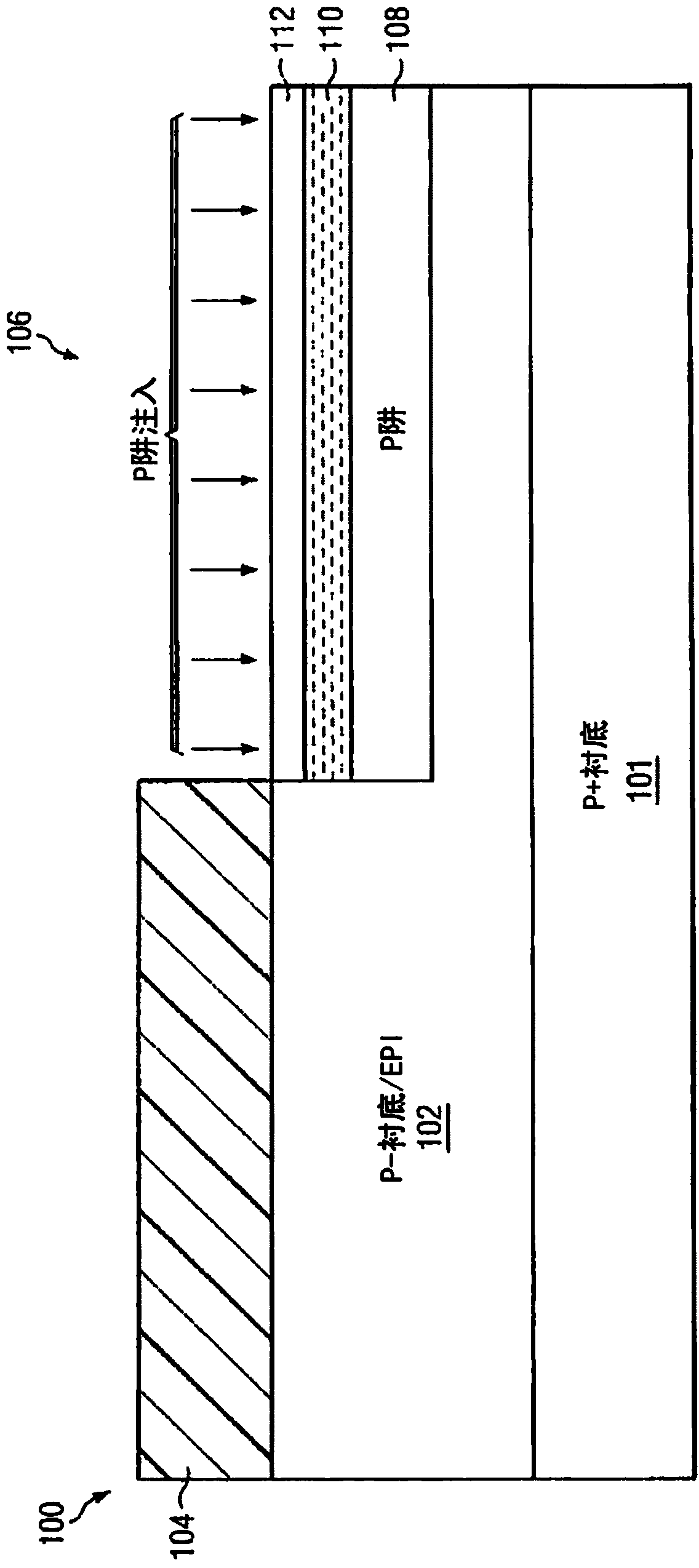
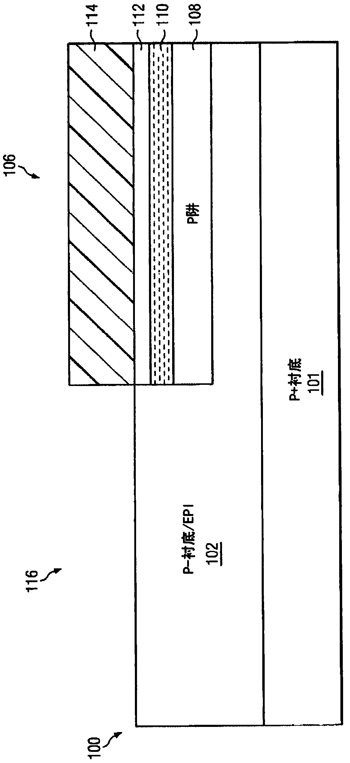
[0023] Various methods can be used to build a transistor element with a channel stack having a shielding layer for shielding the charge on the gate, a threshold voltage control layer for adjusting the threshold voltage of the transistor element, and a layer for high Mobility and reduced random doping fluctuation properties of an intrinsic channel. Each method has different advantages and disadvantages. Typically, two trade-offs are considered when building transistor elements on a semiconductor die, namely the number of steps in the process (related to manufacturing cost) and channel formation (related to transistor performance). Fewer mask steps and total steps needed to build a design translate to lower build costs. Forming the channel late in the thermal cycle of the fabrication process facilitates control of the channel doping profile and avoids the diffusion of undesired contaminants into the channel from other parts of the transistor design.
[0024] Figures 1A to 1K...
PUM
 Abstract
Description
Claims
Application Information
 - R&D Engineer
- R&D Manager
- IP Professional
- Industry Leading Data Capabilities
- Powerful AI technology
- Patent DNA Extraction
Browse by: Latest US Patents, China's latest patents, Technical Efficacy Thesaurus, Application Domain, Technology Topic, Popular Technical Reports.
© 2024 PatSnap. All rights reserved.Legal|Privacy policy|Modern Slavery Act Transparency Statement|Sitemap|About US| Contact US: help@patsnap.com