Array substrate and preparation method and display device of array substrate

A technology of array substrate and substrate substrate, which is applied in semiconductor/solid-state device manufacturing, optics, instruments, etc., can solve the problems of reduced pixel aperture ratio, not very obvious, limited, etc., to improve aperture ratio, reduce resistance value, reduce The effect of voltage differences

Active Publication Date: 2013-12-25
HEFEI BOE OPTOELECTRONICS TECH +1
View PDF7 Cites 26 Cited by
  • Summary
  • Abstract
  • Description
  • Claims
  • Application Information

AI Technical Summary

Problems solved by technology

[0008] In the prior art, since the metal layer 11 and the gate 10 are arranged on the same layer and are made of the same material, the materials used are generally Cr, W, Ti, Ta, Mo, Al, Cu and other metals and their alloys, so that the metal After the layer 11 is connected in parallel with the common electrode layer 20, the resistance of the common electrode layer 20 can be reduced to a certain extent, but due to the restriction of the width d1 of the black matrix 80 on the color filter substrate, and in order to prevent the A short circuit occurs, and the distance between the metal layer 11 and the gate 10 is about 5 micrometers (um), so the width d2 of the metal layer 11 is very limited, so the effect on reducing the resistance of the common electrode layer 20 is not very obvious, However, reducing the resistance of the common electrode layer 20 by increasing the length of d2 will cause d2 to enter the interior of BB'-CC', resulting in a decrease in the pixel aperture ratio

Method used


Image

  • Array substrate and preparation method and display device of array substrate
  • Array substrate and preparation method and display device of array substrate
  • Array substrate and preparation method and display device of array substrate

Examples


preparation example Construction

[0094] Embodiment 5 of the present invention provides a method for preparing an array substrate, the method comprising:

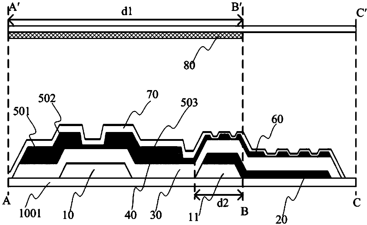
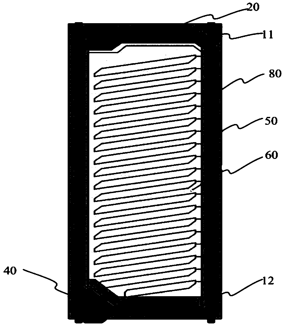
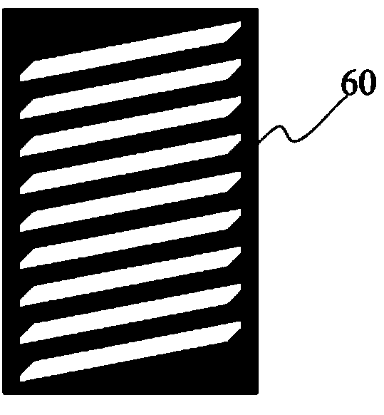
[0095] forming a pattern comprising a common electrode layer and a conductive black matrix on the base substrate, the black matrix is ​​electrically connected to the common electrode layer, and the black matrix is ​​arranged in a non-display area of ​​the pixel unit;

[0096] Forming a second insulating layer on the base substrate, the covered area of ​​the second insulating layer overlaps with the covered area of ​​the black matrix and the common electrode layer, and is used to connect the black matrix and the common electrode layer with the thin film transistor insulation;

[0097] Patterns including thin film transistors and pixel electrodes are formed on the base substrate.

[0098] The array substrate prepared by the method includes a conductive black matrix disposed above the base substrate, the black matrix is ​​electrically connected to the common ...


PUM

PropertyMeasurementUnit
thicknessaaaaaaaaaa

Abstract

The invention provides an array substrate and a preparation method and display device of the array substrate, which are used for reducing the voltage difference of common electrode layers among different pixel units, and increasing the pixel aperture ratio. The array substrate comprises a substrate, grid lines arranged on the substrate in an intersecting way, data lines, and pixel units which are formed by the division of the grid lines and the data lines and are in matrix arrangement, wherein thin film transistors, pixel electrodes and common electrode layers are arranged in the pixel units, and the thin film transistors comprise grid electrodes, first insulating layers, source electrodes, drain electrodes and active layers. The array substrate also comprises black matrixes with conductivity, which are arranged in non-display areas of the pixel units and electrically connected with the common electrode layers, and second insulating layers which are used for insulating the black matrixes and the common electrode layers from the thin film transistors, wherein the coverage areas of the second insulating layers are overlapped with the coverage areas of the black matrixes and the common electrode layers.

Description

technical field [0001] The invention relates to the technical field of liquid crystal display, in particular to an array substrate, a preparation method thereof, and a display device. Background technique [0002] Thin Film Transistor Liquid Crystal Display (TFT-LCD) has the characteristics of small size, low power consumption, and no radiation. It has developed rapidly in recent years and occupies a dominant position in the current flat panel display market. TFT-LCD has been widely used in various large, medium and small size products, almost covering the main electronic products in today's information society, such as LCD TV, high-definition digital TV, computer, mobile phone, vehicle display, projection display, video camera , digital cameras, electronic watches, calculators, electronic instruments, meters, public displays and virtual displays, etc. [0003] TFT-LCD is composed of liquid crystal display panel, driving circuit and backlight module, and liquid crystal disp...

Claims


Application Information

Patent Timeline
Patent Type & Authority Applications(China)
IPC IPC(8): H01L27/12H01L21/77G02F1/1362G02F1/1368G02F1/1333
CPCH01L27/124G02F1/136209H01L27/1248H01L29/78633
Inventor 姜清华秦锋李小和刘永邵贤杰
Owner HEFEI BOE OPTOELECTRONICS TECH
Why Eureka
Try Eureka