

Device for improving luminous efficiency of silicon nitride-based thin-film light-emitting diode and preparation method of device
A technology of light-emitting diodes and silicon nitride films, applied in semiconductor devices, electrical components, circuits, etc., can solve the problems of reducing the injection barrier, unfavorable for light output, and reducing the surface emission efficiency of light, and achieves improved luminous intensity, Achieve the effect of silicon-based monolithic optoelectronic integration and improved luminous efficiency
- Summary
- Abstract
- Description
- Claims
- Application Information
AI Technical Summary
Problems solved by technology
Method used
Image

Examples
Embodiment 1
[0030] The specific steps of the method for improving the luminous efficiency of silicon nitride-based thin-film light-emitting diodes in this embodiment are as follows:
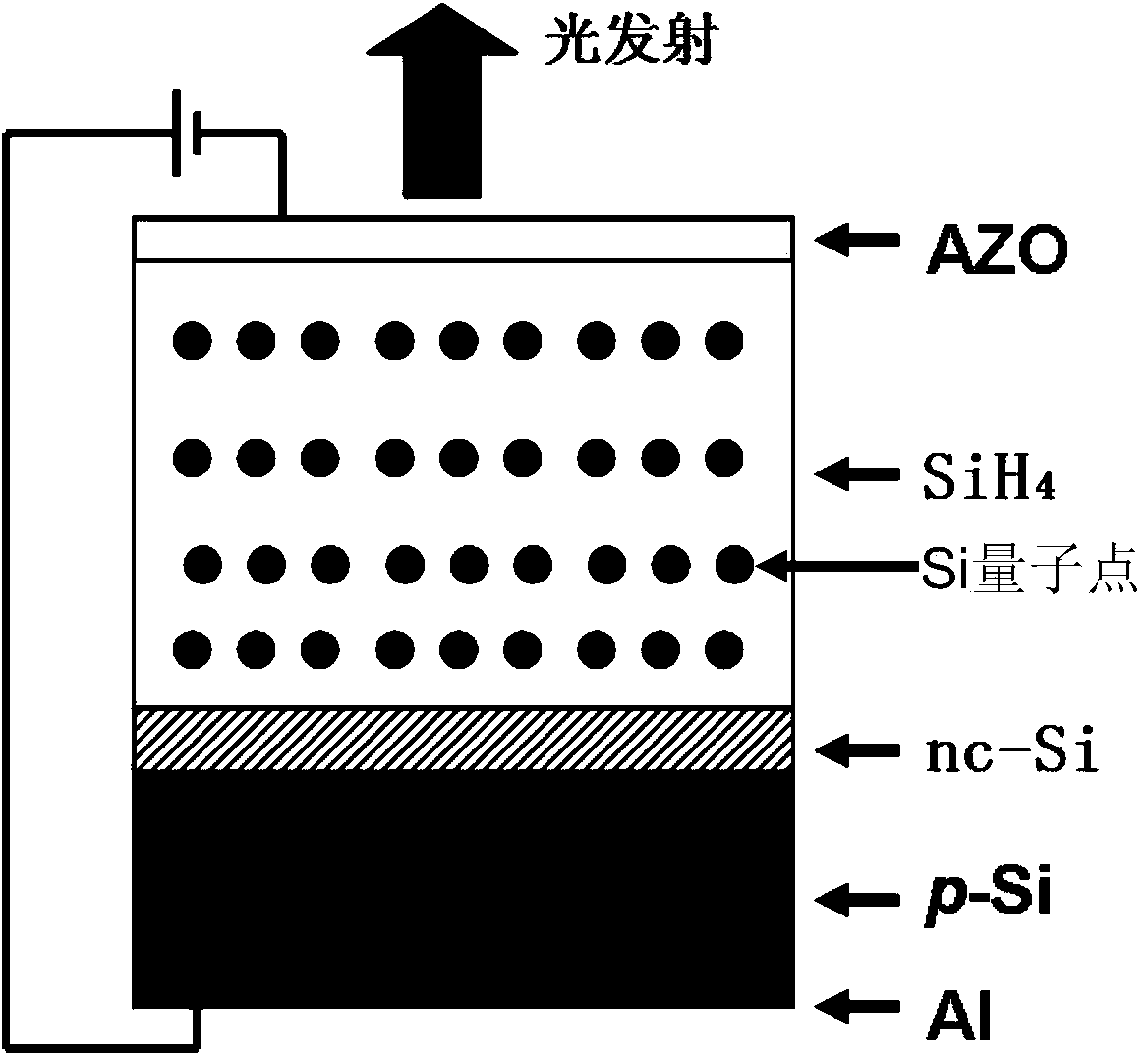
[0031] The first step is to use the parallel plate capacitive radio frequency plasma enhanced chemical vapor deposition method to inject SiH 4 and H 2 gas, depositing a 5nm-thick hydrogen-containing amorphous silicon (a-Si:H) film on a p-Si substrate; the specific equipment control parameters are: RF source power 30W, temperature: 250±10°C, SiH 4 Flow: 1.5sccm, H 2 The flow rate is controlled at 10 sccm, the air pressure is controlled at 60 Pa, and the deposition time is controlled at 75 seconds.
[0032] The second step, after forming a-Si:H thin film, pass SiH 4, NH 3 and H 2 gas, on the a-Si:H film, deposit 50nm thick silicon nitride (SiN x :H) The thin film is used as the light-emitting active layer; the specific equipment control parameters are: the specific equipment control parameters are: RF so...
Embodiment 2
[0041] In this embodiment, the luminous efficiency of silicon nitride-based thin-film light-emitting diodes is improved through the following steps:
[0042] The first step is to use the parallel plate capacitive radio frequency plasma enhanced chemical vapor deposition method to inject SiH 4 and H 2 Gas, deposit 10nm-thick hydrogen-containing amorphous silicon (a-Si:H) film on the p-Si substrate; the specific equipment control parameters are: RF source power 30W, temperature: 250±10°C, SiH 4 Flow: 1.5sccm, H 2 The flow rate is controlled at 10 sccm, the air pressure is controlled at 60 Pa, and the deposition time is controlled at 150 seconds.
[0043] The second step, after forming a-Si:H thin film, pass SiH 4 , NH 3 and H 2 gas, on the a-Si:H film, deposit 50nm thick silicon nitride (SiN x :H) The thin film is used as the light-emitting active layer; the specific equipment control parameters are: the specific equipment control parameters are: RF source power 30W, tempe...
Embodiment 3
[0048] In this embodiment, the luminous efficiency of silicon nitride-based thin-film light-emitting diodes is improved through the following steps:
[0049] The first step is to use the parallel plate capacitive radio frequency plasma enhanced chemical vapor deposition method to inject SiH 4 and H 2 Gas, deposit a 20nm thick hydrogen-containing amorphous silicon (a-Si:H) film on a p-Si substrate; the specific equipment control parameters are: RF source power 30W, temperature: 250±10°C, SiH 4 Flow: 1.5sccm, H 2 The flow rate is controlled at 10 sccm, the air pressure is controlled at 60 Pa, and the deposition time is controlled at 300 seconds.
[0050] The second step, after forming a-Si:H thin film, pass SiH 4 , NH 3 and H 2 gas, on the a-Si:H film, deposit 50nm thick silicon nitride (SiN x :H) The thin film is used as the light-emitting active layer; the specific equipment control parameters are: the specific equipment control parameters are: RF source power 30W, tempe...
PUM
| Property | Measurement | Unit |
|---|---|---|
| thickness | aaaaa | aaaaa |
| thickness | aaaaa | aaaaa |
| thickness | aaaaa | aaaaa |
Abstract
Description
Claims
Application Information