
Device and preparation method for improving luminous efficiency of silicon nitride-based thin-film light-emitting diodes

A technology of silicon nitride film and light-emitting diodes, which is applied in semiconductor devices, electrical components, circuits, etc., can solve the problems of reducing the injection barrier, unfavorable light output, and reducing the surface emission efficiency of light, so as to achieve the improvement of luminous intensity, Achieve silicon-based monolithic optoelectronic integration and improve luminous efficiency

Inactive Publication Date: 2015-11-04
HANSHAN NORMAL UNIV
View PDF6 Cites 0 Cited by
  • Summary
  • Abstract
  • Description
  • Claims
  • Application Information

AI Technical Summary

Problems solved by technology

[0004] The method proposed by many research groups at home and abroad to improve silicon nitride-based light-emitting diodes is mainly to reduce the electron injection barrier by selecting calcium and other low work function metals as the cathode of the device, thereby improving the electron injection efficiency (Appl. Phys .Lett., vol.86, pp.193506, 2005. and Appl.Phys.Lett., vol.89, pp.063509, 2006), but the use of metal instead of ITO (AZO) as the cathode is not conducive to the output of light, The surface emission efficiency of light is reduced, which becomes a stumbling block to improve the luminous efficiency of the device

Method used


Image

  • Device and preparation method for improving luminous efficiency of silicon nitride-based thin-film light-emitting diodes
  • Device and preparation method for improving luminous efficiency of silicon nitride-based thin-film light-emitting diodes
  • Device and preparation method for improving luminous efficiency of silicon nitride-based thin-film light-emitting diodes

Examples


Embodiment 1

[0030] The specific steps of the method for improving the luminous efficiency of the silicon nitride-based thin-film light-emitting diode in this embodiment are as follows:

[0031] The first step is to use the parallel plate capacitive radio frequency plasma enhanced chemical vapor deposition method to pass SiH 4 And H 2 Gas, deposit a hydrogen-containing amorphous silicon (a-Si:H) film with a thickness of 5nm on the p-Si substrate; the specific equipment control parameters are: RF source power 30W, temperature: 250±10℃, SiH 4 Flow rate: 1.5sccm, H 2 The flow rate is controlled at 10 sccm, the air pressure is controlled at 60 Pa, and the deposition time is controlled at 75 seconds.

[0032] The second step, after forming a-Si:H film, pass in SiH 4 , NH 3 And H 2 Gas, on the a-Si:H film, deposit 50nm thick silicon nitride (SiN x :H) Thin film is used as the light-emitting active layer; the specific equipment control parameters are: the specific equipment control parameters are: RF so...

Embodiment 2

[0041] In this embodiment, the luminous efficiency of the silicon nitride-based thin film light-emitting diode is improved by the following steps:

[0042] The first step is to use the parallel plate capacitive radio frequency plasma enhanced chemical vapor deposition method to pass SiH 4 And H 2 Gas, deposit a hydrogen-containing amorphous silicon (a-Si:H) film with a thickness of 10nm on the p-Si substrate; the specific equipment control parameters are: RF source power 30W, temperature: 250±10℃, SiH 4 Flow rate: 1.5sccm, H 2 The flow rate is controlled at 10 sccm, the air pressure is controlled at 60 Pa, and the deposition time is controlled at 150 seconds.

[0043] The second step, after forming a-Si:H film, pass in SiH 4 , NH 3 And H 2 Gas, on the a-Si:H film, deposit 50nm thick silicon nitride (SiN x :H) Thin film is used as the light-emitting active layer; the specific equipment control parameters are: the specific equipment control parameters are: RF source power 30W, temperat...

Embodiment 3

[0048] In this embodiment, the luminous efficiency of the silicon nitride-based thin film light-emitting diode is improved by the following steps:

[0049] The first step is to use the parallel plate capacitive radio frequency plasma enhanced chemical vapor deposition method to pass SiH 4 And H 2 Gas, deposit a hydrogen-containing amorphous silicon (a-Si:H) film with a thickness of 20nm on the p-Si substrate; the specific equipment control parameters are: RF source power 30W, temperature: 250±10℃, SiH 4 Flow rate: 1.5sccm, H 2 The flow rate is controlled at 10 sccm, the air pressure is controlled at 60 Pa, and the deposition time is controlled at 300 seconds.

[0050] The second step, after forming a-Si:H film, pass in SiH 4 , NH 3 And H 2 Gas, on the a-Si:H film, deposit 50nm thick silicon nitride (SiN x :H) Thin film is used as the light-emitting active layer; the specific equipment control parameters are: the specific equipment control parameters are: RF source power 30W, temperat...


PUM

PropertyMeasurementUnit
thicknessaaaaaaaaaa
thicknessaaaaaaaaaa
thicknessaaaaaaaaaa

Abstract

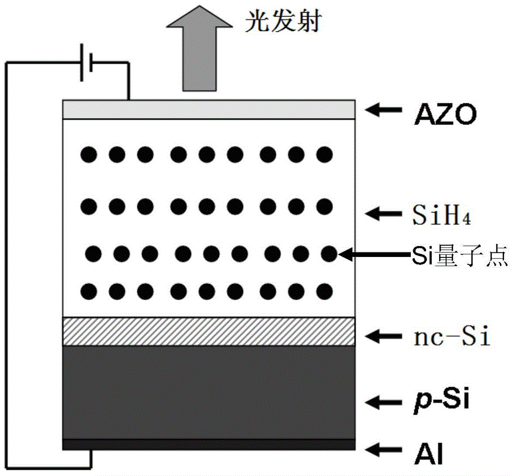
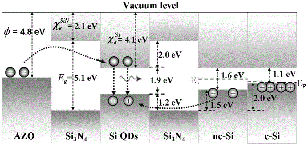
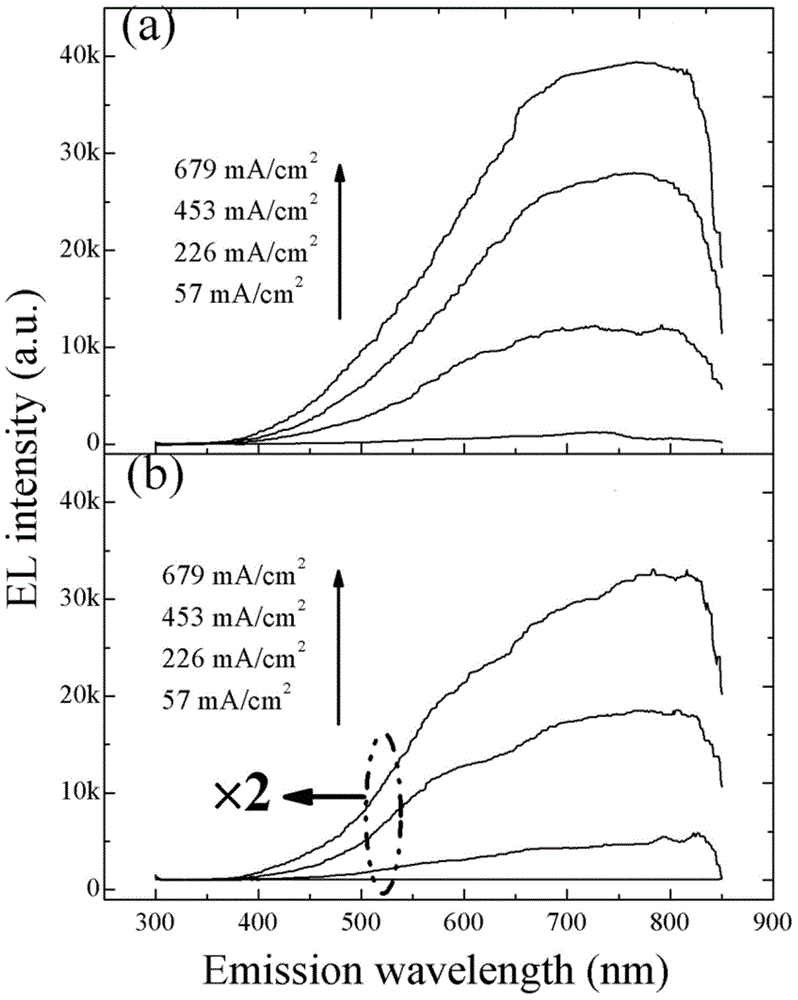
The invention discloses a device for improving the luminous efficiency of a silicon nitride-based thin-film light-emitting diode and a preparation method of the device, and belongs to the technical field of semiconductor luminescent devices. The preparation method mainly comprises the following steps: a p-Si layer is used as a hole-injection layer, and an ultrathin noncrystalline silicon thin film is deposited on the hole-injection layer; a silicon nitride-based thin film is deposited on the ultrathin noncrystalline silicon thin film to serve as a light-emitting active layer; the ultrathin noncrystalline silicon thin film is placed in an annealing furnace to be subjected to dehydrogenation annealing and steady state high temperature annealing in sequence, so that the ultrathin noncrystalline silicon thin film is converted into a nanometer silicon thin film; then, an AZO transparent conducting thin film provided with an optical window is deposited on the silicon nitride-based light-emitting active layer. The device for improving the luminous efficiency of the silicon nitride-based thin-film light-emitting diode and the preparation method of the device mainly have the advantages that ultrathin nanometer silicon is used as a hole blocking layer in the device to effectively restrain hole carriers from being injected excessively, therefore, balanced injection of electrons and holes is promoted, and the luminous efficiency of the device is improved. The preparation process is simple, good in controllability, and compatible with a current microelectronic process.

Description

Technical field [0001] The invention relates to a device for improving the luminous efficiency of a silicon nitride-based thin-film light-emitting diode and a preparation method thereof, in particular to a device using ultrathin nano silicon as a hole blocking layer to suppress excessive injection of hole carriers in a light-emitting device, This promotes the balanced injection of electrons and holes and improves the luminous efficiency of the device. It belongs to the technical field of semiconductor light emitting devices. Background technique [0002] Optoelectronic integration based on semiconductor silicon-based materials is the core of a new generation of semiconductor devices in the 21st century and the hardware foundation of modern information technology. The silicon-based light source is the core and one of the most basic elements for realizing Si monolithic optoelectronic integration. This is not only a major research topic in the current materials science and microele...

Claims


Application Information

Patent Timeline
Patent Type & Authority Patents(China)
IPC IPC(8): H01L33/06H01L33/02H01L33/00
Inventor 黄锐林泽文林圳旭宋超王祥郭艳青宋捷
Owner HANSHAN NORMAL UNIV
Learn More