High-efficiency organic single-layer light-emitting diode and preparation method thereof
A light-emitting diode, high-efficiency technology, used in semiconductor/solid-state device manufacturing, electrical components, electrical solid-state devices, etc., can solve problems such as reducing device efficiency, achieve balanced injection and transmission, improve performance, and improve efficiency.
- Summary
- Abstract
- Description
- Claims
- Application Information
AI Technical Summary
Problems solved by technology
Method used
Image
Examples
Embodiment 1
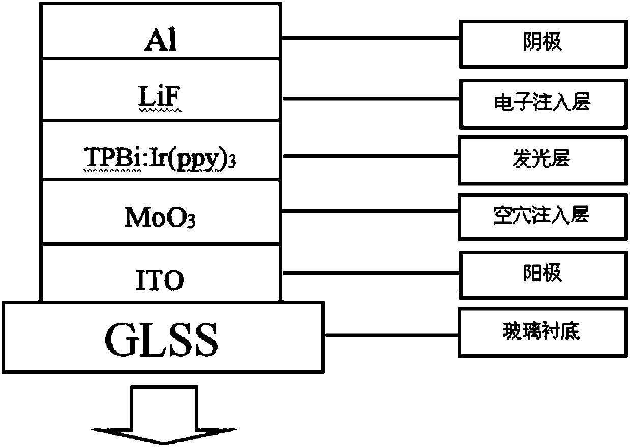
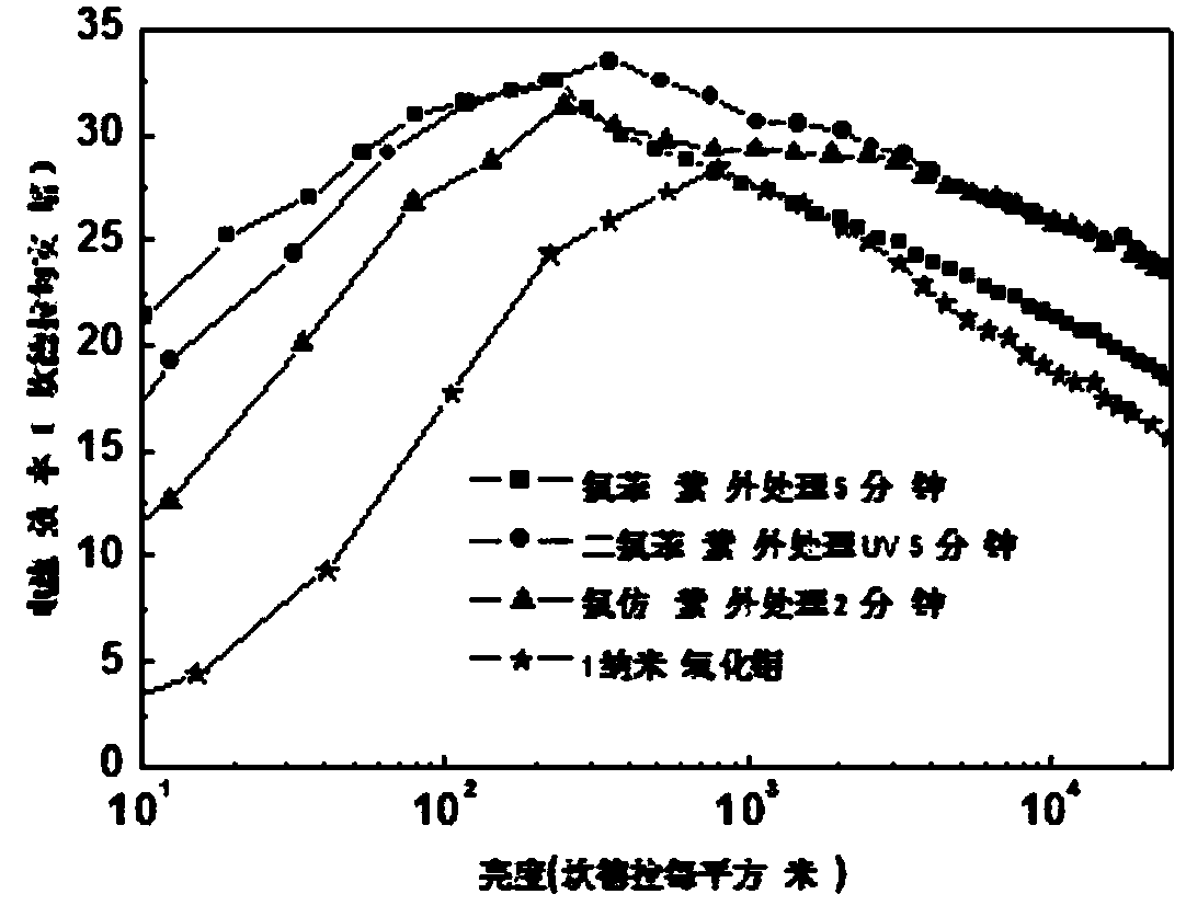
[0034] Sonicate the etched ITO conductive glass twice for 15 minutes with the lotion solution, deionized water, acetone, and ethanol in sequence. After the cleaned ITO conductive glass is blown dry with nitrogen, it is placed in an ultraviolet ozone instrument for 5 minutes, and finally the glass substrate is placed in a vacuum coating system. The organic material is placed in different evaporation sources, and the temperature of each evaporation source can be controlled individually. When the vacuum degree of the vacuum coating system reaches 5×10 -4 When below Pascal, a 1 nm hole injection layer MoO is evaporated on the anode 3 , 100nm light-emitting layer TPBi: Ir(ppy) 3 ,Ir(ppy) 3 The mass fraction of the light-emitting layer accounts for 33% of the mass of the entire light-emitting layer, the electron injection layer LiF of 0.7 nanometers and the thick metal cathode Al of 150 nanometers, and the part where the two electrodes intersect each other forms the light-emittin...
Embodiment 2
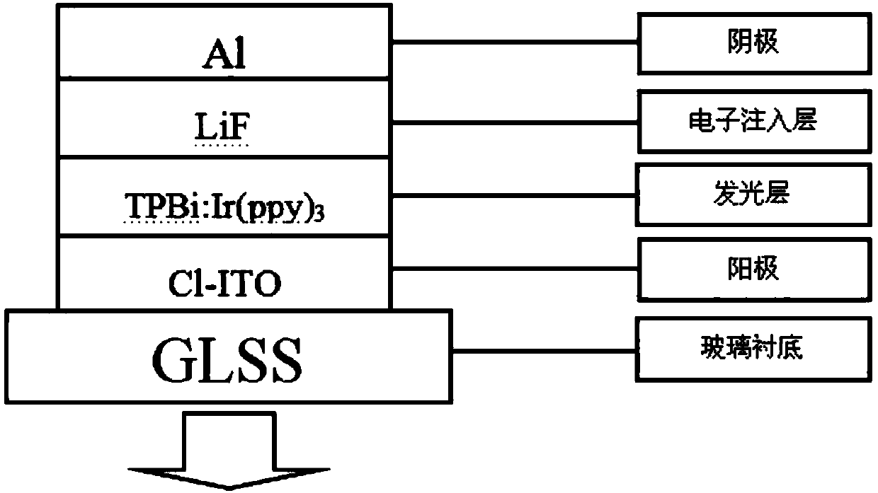
[0036]Sonicate the etched ITO conductive glass twice for 15 minutes with the lotion solution, deionized water, acetone, and ethanol in sequence. After the cleaned ITO conductive glass is blown dry with nitrogen, place it in a UV ozone instrument for 5 minutes, then put the pretreated ITO glass and chloroform solvent into a closed glass reactor, and then treat it with UV for 2 minutes . Finally, put the glass substrate into the vacuum coating system. The organic material is placed in different evaporation sources, and the temperature of each evaporation source can be controlled individually. When the vacuum degree of the vacuum coating system reaches 5×10 -4 Below Pascal, on the anode, 90nm light-emitting layer TPBi: Ir(ppy) 3 ,Ir(ppy) 3 The mass fraction of the light-emitting layer accounts for 33% of the mass of the entire light-emitting layer, the electron injection layer LiF of 0.7 nanometers and the thick metal cathode Al of 150 nanometers, and the part where the two e...
Embodiment 3
[0038] Sonicate the etched ITO conductive glass twice for 15 minutes with the lotion solution, deionized water, acetone, and ethanol in sequence. After the cleaned ITO conductive glass is blown dry with nitrogen, it is placed in a UV ozone instrument for 5 minutes, and then the pretreated ITO glass and chlorobenzene solvent are put into a closed glass reaction kettle together, and then UV treatment is carried out for 5 minutes. minute. Finally, put the glass substrate into the vacuum coating system. The organic material is placed in different evaporation sources, and the temperature of each evaporation source can be controlled individually. When the vacuum degree of the vacuum coating system reaches 5×10 -4 Below Pascal, on the anode, 90nm light-emitting layer TPBi: Ir(ppy) 3 ,Ir(ppy) 3 The mass fraction of the light-emitting layer accounts for 33% of the mass of the entire light-emitting layer, the electron injection layer LiF of 0.7 nanometers and the thick metal cathode...
PUM
 Abstract
Description
Claims
Application Information
 - R&D
- Intellectual Property
- Life Sciences
- Materials
- Tech Scout
- Unparalleled Data Quality
- Higher Quality Content
- 60% Fewer Hallucinations
Browse by: Latest US Patents, China's latest patents, Technical Efficacy Thesaurus, Application Domain, Technology Topic, Popular Technical Reports.
© 2025 PatSnap. All rights reserved.Legal|Privacy policy|Modern Slavery Act Transparency Statement|Sitemap|About US| Contact US: help@patsnap.com


