
A kind of tungsten-copper alloy surface nanometerization method

A tungsten-copper alloy and nanotechnology, which is applied in the field of material surface treatment, can solve problems such as partial surface melting and material failure, and achieve the effects of reduced cut-off value, low cost, and simple operation

Active Publication Date: 2016-04-06
盐城市双新建设投资有限公司
View PDF2 Cites 0 Cited by
  • Summary
  • Abstract
  • Description
  • Claims
  • Application Information

AI Technical Summary

Problems solved by technology

[0003] The purpose of the present invention is to provide a method for surface nanometerization of tungsten-copper alloys, which solves the problem that the existing tungsten-copper alloys are concentrated on the surface of the material by strong arcs generated during the opening and closing process due to high voltage and high current, resulting in serious local melting on the surface. The problem of premature material failure caused by the formation of ablation pits

Method used

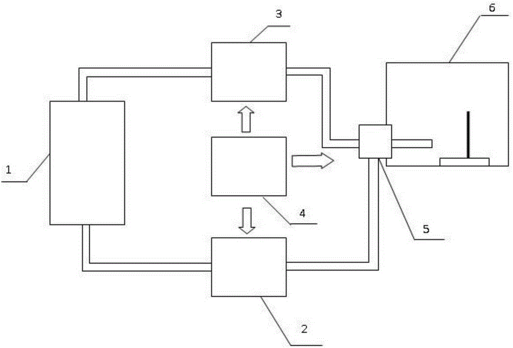

Image

  • A kind of tungsten-copper alloy surface nanometerization method
  • A kind of tungsten-copper alloy surface nanometerization method

Examples


Embodiment 1

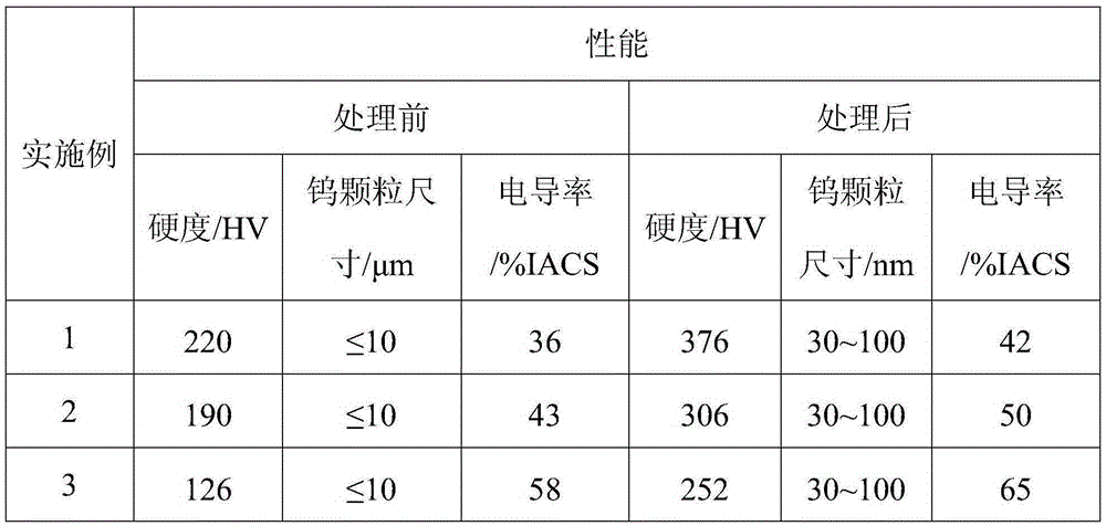
[0028] Step 1, mechanically polishing the surface of the tungsten-copper alloy with a copper content of 20% and cleaning the surface oil with acetone;

[0029] Step 2, place the tungsten-copper alloy pretreated in step 1 in a supersonic particle bombardment device for surface nano-treatment; the process parameters are: gas (air) pressure of 3.5MPa, hard particle size of 0.3mm, hard The particle flow rate is 25g / s, the hard particles are S110 stainless steel, the voltage is 30V, and the processing time is 10min;

[0030] Step 3, place the tungsten-copper alloy that has been treated with surface nanometerization in step 2 in a vacuum furnace, and the vacuum degree is 1×10 -3 Pa, annealing temperature 200°C, and annealing time 30 minutes can be used for stress relief annealing.

[0031] The thickness of the nano-layer on the surface of the tungsten-copper alloy obtained in Example 1 is 0.45 mm.

Embodiment 2

[0033] Step 1, mechanically polishing the surface of a tungsten-copper alloy with a copper content of 30% and cleaning the surface with acetone to remove oil stains;

[0034] Step 2, place the tungsten-copper alloy pretreated in step 1 in a supersonic particle bombardment device for surface nano-treatment; the process parameters are: gas (nitrogen) pressure 2.5MPa, hard particle size 0.3mm, hard The particle flow rate is 20g / s, the hard particles are S110 stainless steel, the voltage is 20V, and the processing time is 60min;

[0035] Step 3, place the tungsten-copper alloy that has been treated with surface nanometerization in step 2 in a vacuum furnace, and the vacuum degree is 1×10 -3 Pa, annealing temperature 200°C, and annealing time 30 minutes can be used for stress relief annealing.

[0036] The thickness of the nano-layer on the surface of the tungsten-copper alloy obtained in Example 2 is 0.8 mm.

Embodiment 3

[0038] Step 1, mechanically polish the surface of the tungsten-copper alloy with a copper content of 50% and clean the surface oil with alcohol;

[0039] Step 2, place the tungsten-copper alloy pretreated in step 1 in a supersonic particle bombardment device for surface nano-treatment; the process parameters are: gas (air) pressure 1.5MPa, hard particle size 0.3mm, hard particle The flow rate is 15g / s, and the hard particles are α-Al 2 o 3 , voltage 20V, processing time 45min;

[0040] Step 3, place the tungsten-copper alloy that has been treated with surface nanometerization in step 2 in a vacuum furnace, and the vacuum degree is 1×10 -3 Pa, annealing temperature 200°C, and annealing time 30 minutes can be used for stress relief annealing.

[0041] The thickness of the nano-layer on the surface of the tungsten-copper alloy obtained in Example 3 is 1.1 mm.


PUM

PropertyMeasurementUnit
thicknessaaaaaaaaaa
thicknessaaaaaaaaaa
thicknessaaaaaaaaaa

Abstract

The invention discloses a nanocrystallization method for a surface of a tungsten-copper alloy. The nanocrystallization method comprises the steps that the pretreated tungsten-copper alloy is put into a supersonic particle bombardment device to carry out surface nanocrystallization, and then stress relief annealing is carried out. By adopting the nanocrystallization method for the surface of the tungsten-copper alloy disclosed by the invention, surface nanocrystallization and stress relief annealing are orderly carried out on the pretreated tungsten-copper alloy, so that the grain size of the surface of the tungsten-copper alloy can be greatly refined; a nano structure with a certain depth and even tungsten / copper dual-phase distribution is formed on the alloy surface; the thickness of a nano layer on the surface of the tungsten-copper alloy is 0.3-1.2mm; the surface hardness of a tungsten-copper electric contact material is significantly improved; the characteristics of arc ablation resistance and the breakdown voltage are obviously improved; the cut-off value is greatly reduced; the nanocrystallization method is simple to operate, less in energy consumption, low in cost, high in production efficiency and easy for industrial production.

Description

technical field [0001] The invention belongs to the technical field of material surface treatment, and relates to a method for nanometerizing the surface of a tungsten-copper alloy. Background technique [0002] Tungsten-copper alloy has the properties of high temperature resistance, arc ablation resistance, fusion welding resistance, small cut-off current, low thermal electron emission ability, etc., and is widely used in electrical contact materials and high temperature resistant parts in aerospace. Although tungsten copper alloy has been widely used, its performance still needs to be improved. When tungsten-copper alloy is used as an electrical contact material in service, the strong arc generated by high voltage and high current during the switching process gathers on the surface of the material, resulting in severe local melting on the surface, forming ablation pits and causing premature failure of the material. Studies have found that the performance of tungsten-coppe...

Claims


Application Information

Patent Timeline
Patent Type & Authority Patents(China)
IPC IPC(8): C22F3/00
Inventor 陈文革张志军刘冰
Owner 盐城市双新建设投资有限公司
Learn More