Flip Chip Light Emitting Diode and Its Manufacturing Method and Application

A light-emitting diode and flip-chip technology, applied in the field of chip board packaging structure, can solve the problems of inability to achieve light output rate, influence luminous intensity, thermal expansion of materials, etc. The effect of degree and longevity

Active Publication Date: 2016-06-29
RITEDIA CORPORATION
View PDF6 Cites 2 Cited by
  • Summary
  • Abstract
  • Description
  • Claims
  • Application Information

AI Technical Summary

Problems solved by technology

However, nearly 80% of the current input power of LEDs will be converted into heat energy. If the carrier board carrying the LED components cannot effectively dissipate heat, the temperature of the LED chip interface will increase. In addition to affecting the luminous intensity, It may also cause heat expansion of each layer of material due to the accumulation of heat in the LED chip, causing damage to the structure and adversely affecting the life of the product. In addition, because the light excited in the LED is diffused in a radiative manner, not all The light will be scattered through the surface of the LED, so the light extraction rate is not good, and the most effective light extraction rate cannot be achieved

Method used


Image

  • Flip Chip Light Emitting Diode and Its Manufacturing Method and Application
  • Flip Chip Light Emitting Diode and Its Manufacturing Method and Application
  • Flip Chip Light Emitting Diode and Its Manufacturing Method and Application

Examples


Embodiment 1

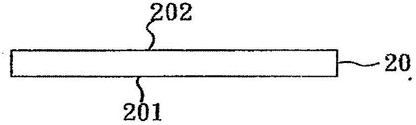
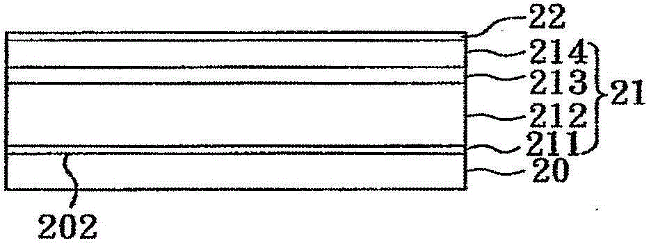
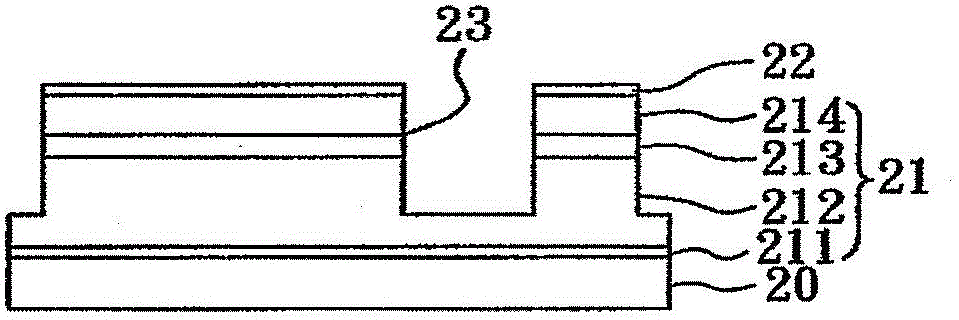
[0075] refer to Figures 1A to 1H It is a schematic flow diagram of the manufacturing method of the flip-chip light emitting diode according to the first embodiment of the present invention. First, if Figure 1A As shown, a substrate 20 is provided, which has a first surface 201 and a second surface 202 opposite to the first surface 201 . Next, if Figure 2B As shown, a semiconductor epitaxial multilayer composite structure 21 is formed above the second surface 202 of the substrate 20, wherein the semiconductor epitaxial multilayer composite structure 21 includes an undoped semiconductor epitaxial layer 211, a first Semiconductor epitaxial layer 212, an active intermediate layer 213, and a second semiconductor epitaxial layer 214, wherein the undoped semiconductor epitaxial layer 211, the first semiconductor epitaxial layer 212, the active intermediate layer 213 and the The second semiconductor epitaxial layer 214 is stacked, the undoped semiconductor epitaxial layer 211 is ...

Embodiment 2

[0085] Please refer to image 3 , a schematic diagram of the structure of the flip-chip light emitting diode according to the second embodiment of the present invention. like image 3 As shown, the structure of the flip-chip light emitting diode of this embodiment is substantially the same as that of the first embodiment, including: a substrate 40 having a first surface 401 and a second surface 402 opposite to the first surface 401; A semiconductor epitaxial multilayer composite structure 41 located on the second surface 402 of the substrate 40 and the semiconductor epitaxial multilayer composite structure 41 includes an undoped semiconductor epitaxial layer 411 and a first semiconductor epitaxial layer 412 , an active intermediate layer 413, and a second semiconductor epitaxial layer 414, wherein the undoped semiconductor epitaxial layer 411, the first semiconductor epitaxial layer 412, the active intermediate layer 413, and the second semiconductor epitaxial layer 414 The ...

Embodiment 3

[0087] refer to Figure 4 , which is a schematic structural diagram of the chip-on-board packaging structure of this embodiment. like Figure 4 As shown, the package structure on the chip includes: a circuit carrier board 6; The circuit carrier board 6 is electrically connected, wherein the circuit carrier board 6 includes an insulating layer 61, a circuit substrate 60, and an electrical connection pad 63, and the material of the insulating layer 61 can be selected from diamond-like carbon, alumina, ceramics, Diamond-containing epoxy resin, or a mixture of the above materials, the circuit substrate 60 is a metal plate, a ceramic plate or a silicon substrate.

[0088] In the chip-on-chip package structure, the solder 62 formed on the surface of the electrical connection pad 63 can be used to connect the first metal bonding layer 29 and the second metal bonding layer 28 to the circuit board through flip chip. The electrical connection pads 63 of 6 are electrically connected. ...


PUM

PropertyMeasurementUnit
refractive indexaaaaaaaaaa

Abstract

A flip-chip light emitting diode is disclosed, and includes: a substrate, a semiconductor multilayer structure, first and second electrodes, first and second diamond-like-carbon / conductive-material composite structures, and a passivation layer, wherein, the passivation layer is a stacked structure possessing a material of different refractive index, and the first and second diamond-like-carbon / conductive-material can buffer thermal stress in the flip-chip light emitting diode. Therefore, the flip-chip light emitting diode can improve the whole photoelectric efficiency, and prevent the photoelectric characteristic of elements from being decreased, and accordingly its reliability and service life are improved. A method of manufacturing the abovementioned flip-chip light emitting diode and application thereof are also disclosed.

Description

technical field [0001] The present invention relates to a flip-chip light-emitting diode, a manufacturing method thereof, and a chip-on-board packaging structure using the same, and more particularly, to a flip-chip light-emitting diode capable of buffering coefficient thermal expansion mismatch and improving output light rate in the structure. A manufacturing method thereof and a chip-on-board packaging structure using the same. Background technique [0002] In 1962, Nick Holonyak Jr. of General Electric Company developed the first practical application of visible light-emitting diodes (LightEmittingDiode, LED), and with the increasing technology update, the development of various color light-emitting diodes has also been applied. and live. Under the premise of today's pursuit of sustainable development, light-emitting diodes have gradually replaced the indicators or indicators used for lighting or various electrical equipment in daily life due to the advantages of low pow...

Claims


Application Information

Patent Timeline
Patent Type & Authority Patents(China)
IPC IPC(8): H01L33/46H01L33/64H01L33/00
CPCH01L33/005H01L33/12H01L33/62
Inventor 甘明吉蔡百扬宋健民
Owner RITEDIA CORPORATION
Why Eureka
Try Eureka