Circuit-board developing, electroplating and etching device

A technology for etching equipment and circuit boards, which is applied in the field of circuit board development, electroplating and etching equipment, can solve the problems of reducing the yield of the circuit board manufacturing process and increasing the cost of the circuit board manufacturing process, and achieves the effect of reducing the impact and improving the yield rate.

Active Publication Date: 2014-01-01
TRIPOD WUXI ELECTRONICS
View PDF3 Cites 5 Cited by
  • Summary
  • Abstract
  • Description
  • Claims
  • Application Information

AI Technical Summary

Problems solved by technology

[0003] Since the production process of the circuit board is through a discontinuous equipment, the circuit board is manually transferred from the developing equipment to the electroplating equipment, from the electroplating equipment to the stripping equipment, and the...

Method used


Image

  • Circuit-board developing, electroplating and etching device
  • Circuit-board developing, electroplating and etching device
  • Circuit-board developing, electroplating and etching device

Examples


Embodiment Construction

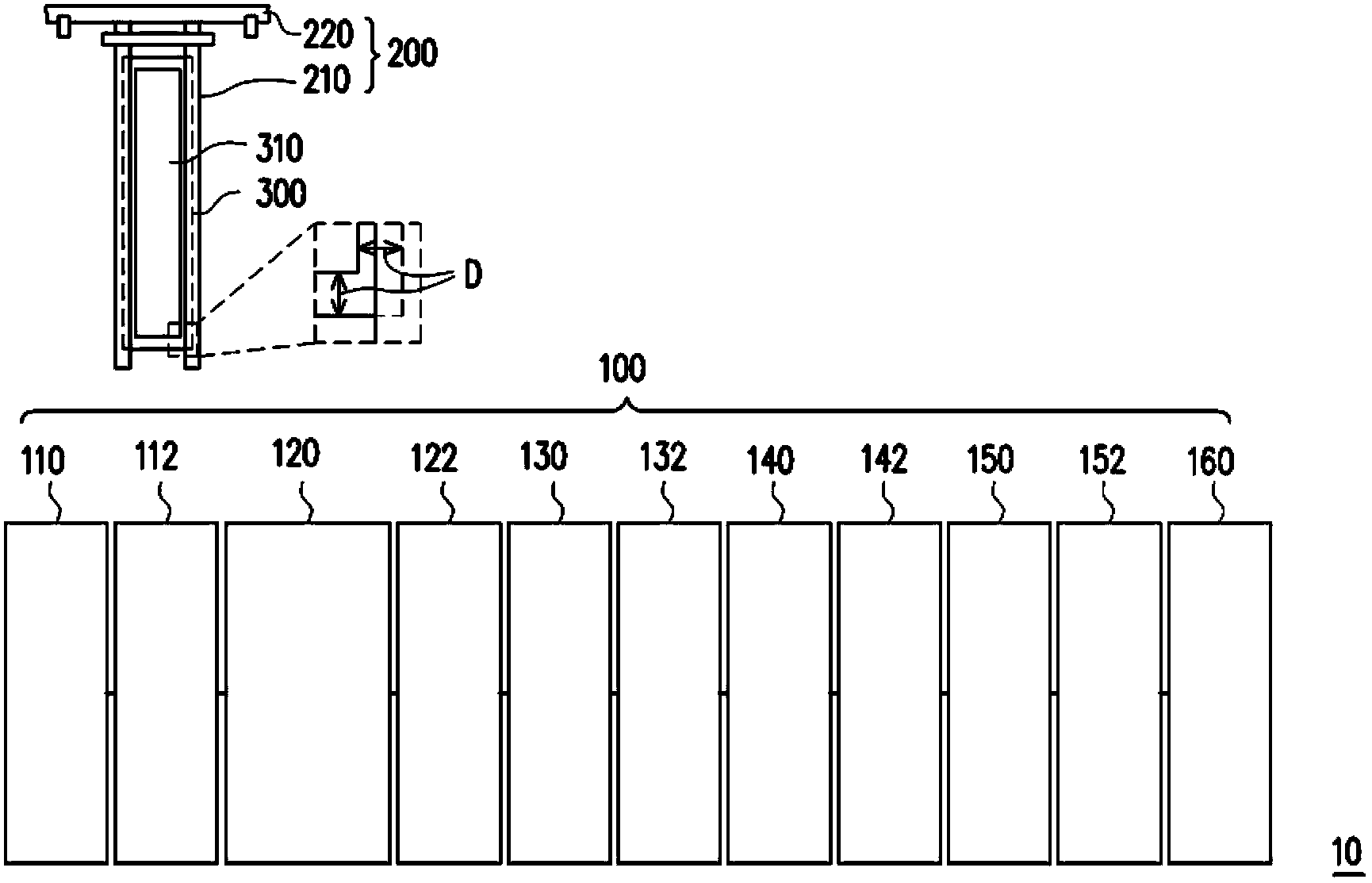
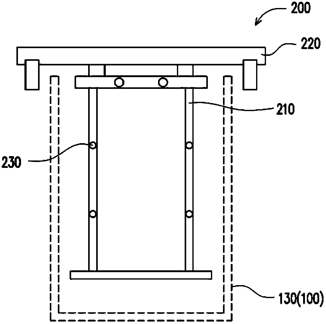
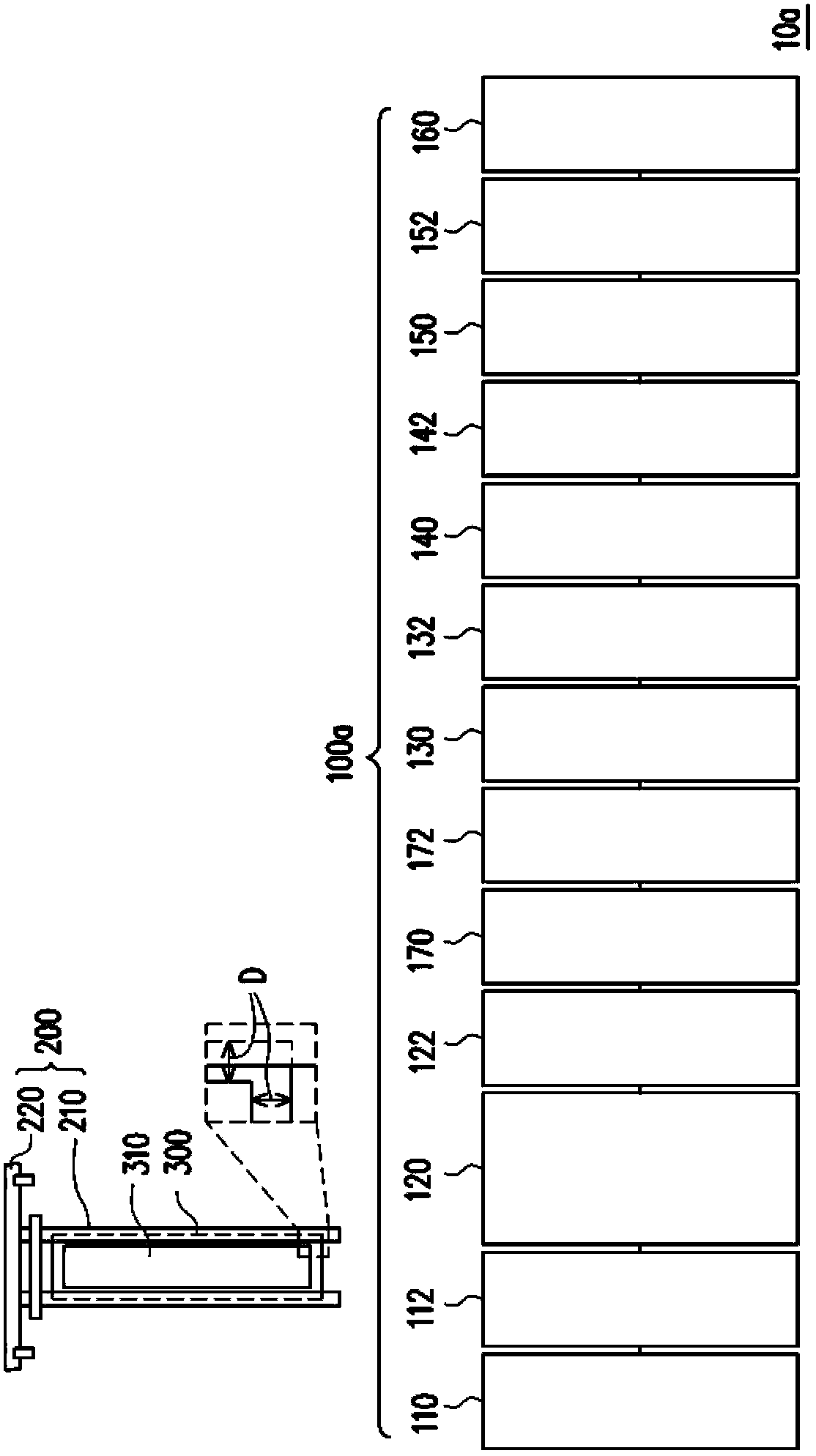
[0045] figure 1 It is a schematic diagram of a circuit board developing, electroplating and etching equipment according to an embodiment of the present invention. figure 2 is a schematic diagram of a mobile unit according to an embodiment of the present invention. Please also refer to figure 1 and figure 2 , in this embodiment, the circuit board developing, electroplating and etching equipment 10 is suitable for developing, electroplating and etching an exposed circuit board 300, wherein the circuit board 300 is, for example, a printed circuit board (Printed Circuit Board, PCB).

[0046] The circuit board developing, electroplating and etching equipment 10 includes a plurality of tank units 100 and a moving unit 200 . Tank unit 100 comprises a developing tank 110, a first washing tank 112, a pickling tank 120, a second washing tank 122, an electroplating tank 130, a third washing tank 132, a stripping tank 140, a fourth washing tank tank 142 , an etching tank 150 , a fif...


PUM


Abstract

The invention discloses a circuit-board developing, electroplating and etching device suitable for carrying out manufacturing processes of developing, electroplating and etching on an exposed circuit board. The circuit-board developing, electroplating and etching device comprises a plurality of tank units and a moving unit. The tank units comprise a developing tank, a first water washing tank, an acid washing tank, a second water washing tank, an electroplating tank, a third water washing tank, a stripping tank, a fourth water washing tank, an etching tank, a fifth water washing tank and a drying tank, wherein the tanks are connected with one another in sequence. The moving unit clamps the exposed circuit board and enables the exposed circuit board to pass through the developing tank, the first water washing tank, the acid washing tank, the second water washing tank, the electroplating tank, the third water washing tank, the stripping tank, the fourth water washing tank, the etching tank, the fifth water washing tank and the drying tank in sequence, and therefore the manufacturing processes of developing, electroplating and etching are completed.

Description

technical field [0001] The invention relates to a manufacturing process equipment, and in particular to a circuit board developing, electroplating and etching equipment. Background technique [0002] As far as the prior art is concerned, the manufacturing process of the circuit board is mainly through steps such as exposure, development, electroplating and etching. Generally speaking, sending the exposed circuit board into developing equipment, electroplating equipment, stripping photoresist equipment, and etching equipment is all moved by manual handling. Therefore, during the transportation process, due to the influence of external environmental factors, there will be dust or oxidation on the circuit board. Therefore, before the circuit board is sent from the development equipment to the electroplating equipment, stripping and etching equipment, the circuit board must first go through the process of water washing to clean the circuit board, or the process of deoxidation t...

Claims


Application Information

Patent Timeline
IPC IPC(8): H05K3/06
Inventor 藤川治孙奇杨中贤杨伟雄
Owner TRIPOD WUXI ELECTRONICS
Why Eureka
Try Eureka