Array substrate, display device and manufacturing method of array substrate

An array substrate and substrate technology, applied in nonlinear optics, instruments, optics, etc., can solve problems such as poor display effect, achieve the effects of reducing jump voltage, improving display effect, and reducing capacitance value

Active Publication Date: 2016-01-06
HEFEI BOE OPTOELECTRONICS TECH +1
View PDF4 Cites 0 Cited by
  • Summary
  • Abstract
  • Description
  • Claims
  • Application Information

AI Technical Summary

Problems solved by technology

However, the change of the gate voltage will cause the pixel electrode to generate jump voltage through the parasitic capacitance, and the magnitude of the jump voltage is proportional to the capacitance value of the parasitic capacitor. Therefore, after the thin film transistor is turned off, the jump voltage will make the actual pixel voltage less than The charging voltage when the thin film transistor is turned on, resulting in poor display effect

Method used


Image

  • Array substrate, display device and manufacturing method of array substrate
  • Array substrate, display device and manufacturing method of array substrate
  • Array substrate, display device and manufacturing method of array substrate

Examples


Embodiment 1

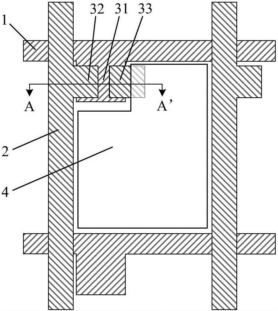
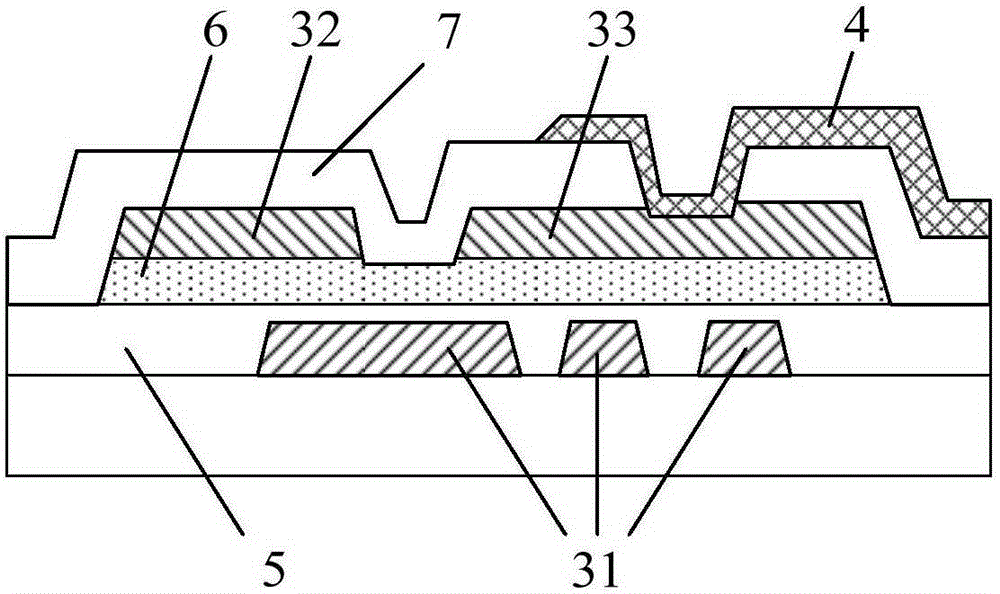
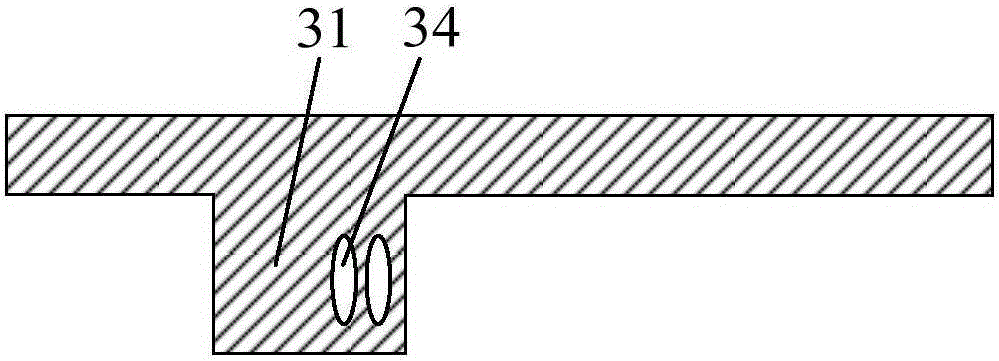
[0029] like figure 1 and figure 2 As shown, this embodiment provides an array substrate, including gate lines 1, data lines 2, thin film transistors and transparent electrodes 4, the thin film transistors include a gate 31, a source 32 and a drain 33, the gate of the above thin film transistor 31 is connected to the gate line 1, the source 32 of the thin film transistor is connected to the data line 2, and the drain 33 of the thin film transistor is connected to the transparent electrode 4, as figure 2 and image 3 As shown, a gate through hole 34 is provided in a region overlapping the drain 33 on the gate 31 . The number, size and shape of the gate through holes 34 are not limited in this implementation.

[0030] In the array substrate in this embodiment, a gate through hole is provided on the gate in the overlapping region of the gate and the drain of the thin film transistor, which reduces the overlapping area of ​​the gate and the drain, thus reducing the gap between...

Embodiment 2

[0032] like Figure 4 As shown, this embodiment provides an array substrate, including a gate line, a data line, a thin film transistor and a transparent electrode 4, the gate 31 of the thin film transistor is connected to the gate line, and the source 32 of the thin film transistor is connected to the data line. line, the drain 33 of the thin film transistor is connected to the transparent electrode 4, the gate 31 includes a first region, the thickness of the gate 31 in the first region is smaller than the thickness of the gate 31 outside the first region, and the first region is located In the overlapping region of the gate 31 and the drain 33 . It should be noted that, this embodiment does not limit the shape of the first region. For example, the area of ​​the first region may be very small, which is equivalent to an unpenetrated through hole; the first region may also be divided into multiple region blocks, and these region blocks may be in the shape of bars, circles, and...

Embodiment 3

[0036] This embodiment provides a display device, including the array substrate in Embodiment 1 or Embodiment 2.

[0037] In the display device in this embodiment, a gate through hole is provided on the gate in the overlapping region of the gate and the drain of the thin film transistor to reduce the area where the gate and the drain overlap, or the gate and the drain overlap The thickness of the gate in the first region is reduced to increase the distance between the gate and the drain in the overlapping region, thereby reducing the capacitance value of the parasitic capacitance formed between the gate and the drain, and reducing the generation of parasitic capacitance The jump voltage, thus improving the display effect.


PUM


Abstract

The invention discloses an array substrate, a display device and a method for manufacturing the array substrate, and relates to the technical field of liquid crystal display. Leaping voltages generated by stray capacitance can be lowered, and therefore the display effect can be improved. The array substrate comprises a grid line, a data line, a thin film transistor and a transparent electrode. The grid electrode of the thin film transistor is connected to the grid line, the source electrode of the thin film transistor is connected to the data line, and the drain electrode of the thin film transistor is connected to the transparent electrode. Grid through holes are formed in the area, overlapping with the drain electrode, in the grid electrode, or the grid electrode comprises a first area, and the thickness of the grid electrode inside the first area is smaller than the thickness of the grid electrode outside the first area. The first area is placed in the area, overlapping with the drain electrode, in the grid electrode.

Description

technical field [0001] The present invention relates to the technical field of liquid crystal display, in particular to an array substrate, a display device and a manufacturing method of the array substrate. Background technique [0002] Thin Film Transistor Liquid Crystal Display (TFT-LCD for short) occupies a dominant position in the display market due to its small size, low power consumption, and no radiation. [0003] In the existing TFT-LCD structure, there is a certain overlapping area between the drain and the gate in the thin film transistor, so that a parasitic capacitance is formed in this area. When the gate voltage controls the thin film transistor to turn on, the data line charges the pixel electrode to the pixel voltage, and when the gate voltage controls the thin film transistor to turn off, the pixel voltage is stored. However, the change of the gate voltage will cause the pixel electrode to generate jump voltage through the parasitic capacitance, and the ma...

Claims


Application Information

Patent Timeline
Patent Type & Authority Patents(China)
IPC IPC(8): G02F1/1368G02F1/1333
Inventor 马俊才
Owner HEFEI BOE OPTOELECTRONICS TECH
Why Eureka
Try Eureka