Splicing-type PCB capable of being broken

A technology of PCB boards and broken lines, applied in the field of spliced ​​PCB boards, can solve problems such as affecting the health of operators, high cost, noise and dust, and polluting the environment, so as to reduce the difficulty of PCB cutting and separation processing, reduce work difficulty, and reduce Effects of Environmental Pollution and Noise Pollution

Inactive Publication Date: 2014-01-15
蒋莺
View PDF0 Cites 1 Cited by
  • Summary
  • Abstract
  • Description
  • Claims
  • Application Information

AI Technical Summary

Problems solved by technology

At the same time, due to the high strength of the base material of the printed circuit board, specific cutting tools are required in the process of cutting, which is costly and causes pollution such as noise and dust, which will affect the health of operators. and pollute the environment

Method used


Image

  • Splicing-type PCB capable of being broken

Examples


Embodiment Construction

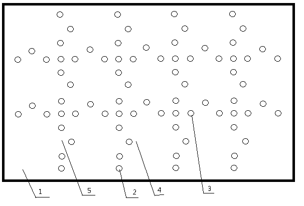
[0016] The present invention will be further explained below in conjunction with the accompanying drawings and specific embodiments. It should be understood that the following specific embodiments are only used to illustrate the present invention and are not intended to limit the scope of the present invention. It should be noted that the words "front", "rear", "left", "right", "upper" and "lower" used in the following description refer to the direction in the figure, and the words "inner" and "outer ” refer to directions towards or away from the geometric center of a particular part, respectively.

[0017] Such as figure 1 As shown, in the breakable splicing PCB board disclosed by the present invention, the substrate 1 is provided with a fracture line, the fracture line includes a longitudinal fracture line 2 and a transverse fracture line 3, and the longitudinal fracture line 2 and the transverse fracture line 3 are formed on the substrate 1. Distributed in a grid shape, th...


PUM


Abstract

The invention discloses a splicing-type PCB capable of being broken. A substrate is provided with a broken line. The broken line comprises a vertical broken line and a transverse broken line. The vertical broken line and a transverse broken line form grid-shape distribution on the substrate. The broken line forms a protruded tongue bending on the substrate. The tongue bending forms a clamping groove and a clamping component on the substrate. By using the PCB of the invention, technical problems are solved; workability and a combination positioning function of the PCB are increased; the PCB can be broken without a specific cutting tool under the condition that intensity and a mechanical property are guaranteed; an operation difficulty of PCB processing is reduced; PCB substrate processing efficiency is effectively increased; subsequent processing cost of the PCB is reduced. Simultaneously, through using the tongue-shaped clamping groove and the clamping component formed by the broken line, combination positioning can be performed on the PCB during splicing; working difficulty is reduced and working efficiency is increased.

Description

[0001] technical field [0002] The invention relates to a printed circuit board, in particular to a breakable spliced ​​PCB board. Background technique [0003] Printed circuit board, also known as printed circuit board, printed circuit board, referred to as printed board, English referred to as PCB (printed circuit board) or PWB (printed wiring board), with insulating board as the base material, cut into a certain size, on it At least one conductive pattern is attached, and holes are arranged (such as component holes, fastening holes, metallized holes, etc.), which are used to replace the chassis of electronic components installed in the past and realize the interconnection between electronic components. Since such boards are made using electronic printing, they are called "printed" circuit boards. It is not accurate to call "printed circuit board" as "printed circuit" because there are no "printed components" on the printed board but only wiring. It is an important ...

Claims


Application Information

Patent Timeline
Patent Type & Authority Applications(China)
IPC IPC(8): H05K1/02
Inventor 蒋莺
Owner 蒋莺
Why Eureka
Try Eureka