In2O3-ZnO sputtering target

A sputtering target, in2o3 technology, applied in the field of sputtering targets, can solve the problems of not increasing the oxygen partial pressure, a large number of carriers, and easy to generate leakage current, etc., and achieve the effect of suppressing the generation of abnormal discharge

Inactive Publication Date: 2014-01-15
IDEMITSU KOSAN CO LTD
View PDF4 Cites 7 Cited by
  • Summary
  • Abstract
  • Description
  • Claims
  • Application Information

AI Technical Summary

Problems solved by technology

However, when the film is formed by the sputtering method generally performed in industry, the oxide semiconductor film containing a crystalline substance mainly composed of zinc oxide has the following problems: it is easy to generate oxygen vacancies, a large number of carriers are generated, and it is difficult to use The conductivity becomes smaller
In addition, when forming a film by the sputtering method, there are problems that abnormal discharge occurs, the stability of film formation is impaired, and the uniformity and reproducibility of the obtained film are lowered.
[0005] In addition, in particular, for an oxide semiconductor film containing a crystalline substance mainly composed of zinc oxide, the field-effect mobility (hereinafter sometimes simply referred to as "mobility") is as low as 1 cm 2 About / V sec, the on / off ratio is small, and it is easy to generate leakage current
Therefore, when an oxide semiconductor film containing a crystalline substance mainly composed of zinc oxide is used as the active layer (channel layer) of the TFT, there is a problem that a large current flows even when no gate voltage is applied. Between the source terminal and the drain terminal, so that the normally-off (normally-off) operation of the TFT cannot be achieved
However, there are problems as follows: Gallium is a rare metal and the cost of raw materials is high. If the amount of gallium added is reduced or the oxygen partial pressure during film formation is not increased, the normally-off operation of TFT cannot be realized.
However, this target has the following problems: it is easy to form aggregates of insulating substances, which increases the resistance value, and it is easy to cause abnormal discharge, etc.

Method used


Image

  • In2O3-ZnO sputtering target
  • In2O3-ZnO sputtering target
  • In2O3-ZnO sputtering target

Examples


Embodiment 1

[0120] (1) Preparation of raw materials

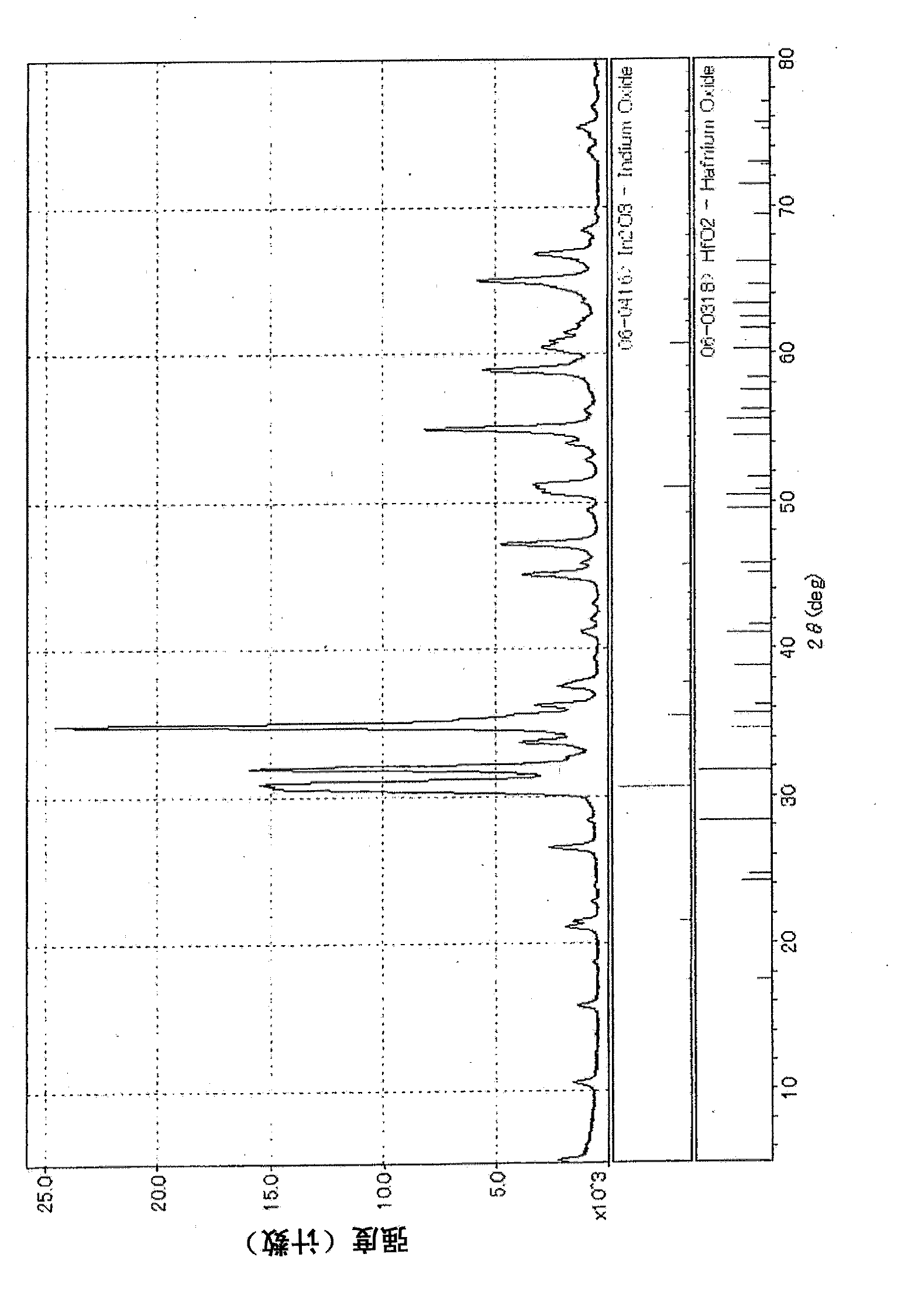
[0121] As raw materials, indium oxide (manufactured by Asia Material Co., Ltd., average particle size: 1 μm or less, purity: 4N equivalent) and hafnium oxide (manufactured by Wako Pure Chemical Industries, Ltd., average particle size: 1 μm or less, purity: 4N equivalent) were used ). These were mixed so that the atomic ratio [In / (In+Hf)] of the In element to the total of the In element and the Hf element was 0.88. The mixture was supplied to a wet ball mill, mixed and pulverized for 12 hours.

[0122] The resulting mixed slurry was removed, filtered and dried. This dried powder was charged into a firing furnace, and heat-treated at 1000° C. for 5 hours in an air atmosphere.

[0123] Through the above steps, a mixed powder containing In element and Hf element is obtained.

[0124] Zinc oxide (manufactured by High Purity Chemical Co., Ltd., average particle diameter: 1 μm or less, purity: 4N equivalent) was mixed with this mixed powd...

Embodiment 2~25

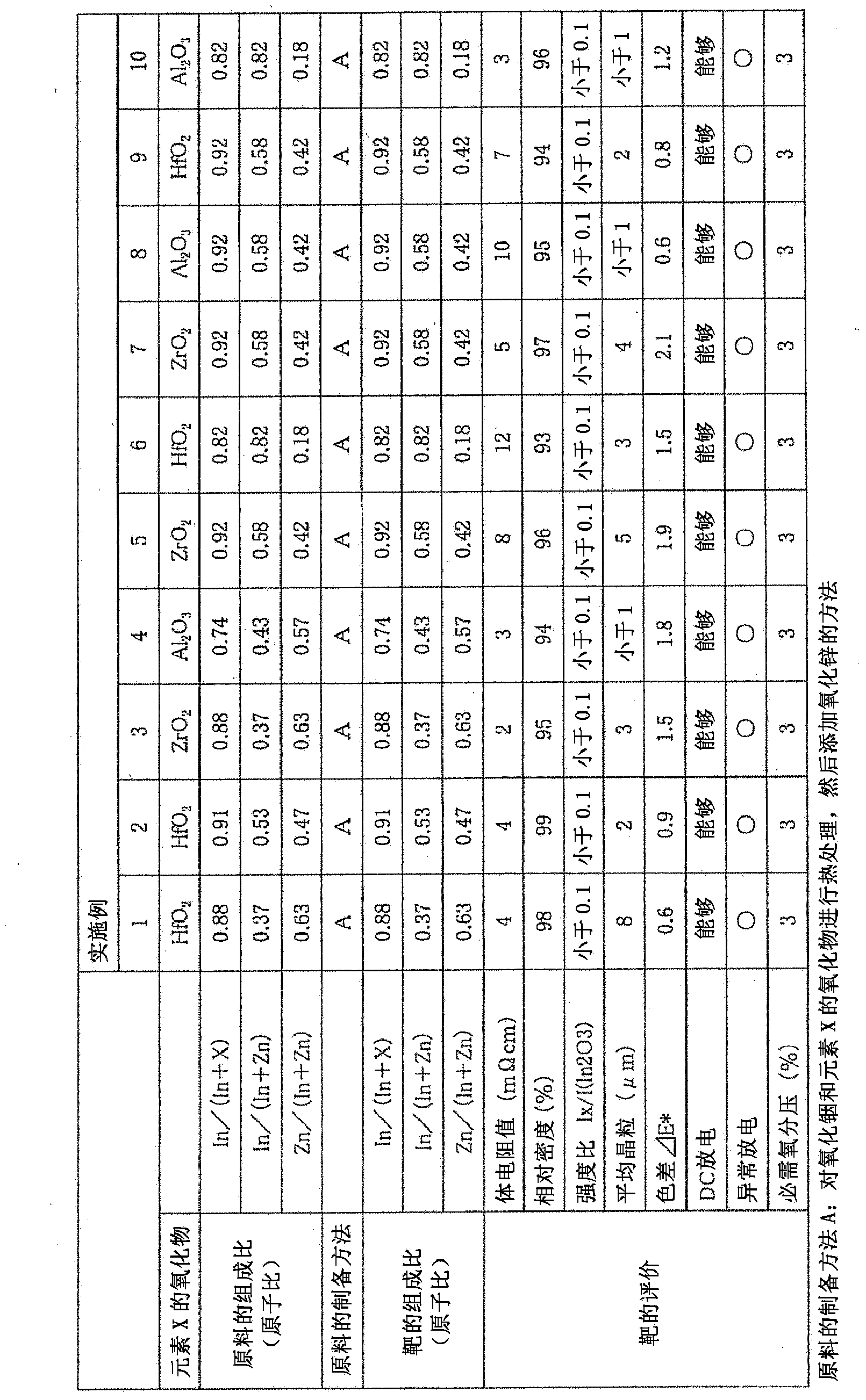
[0167] In preparation of a raw material, except having changed the compounding ratio of a raw material and the oxide of the element X as shown in Table 1 - Table 3, it carried out similarly to Example 1, and produced and evaluated the sputtering target. The results are shown in Tables 1 to 3.

[0168] It should be noted that the oxides of the element X used were all manufactured by Wako Pure Chemical Industries, Ltd.

Embodiment 26~29

[0170] Indium oxide, zinc oxide, and oxides of element X were weighed in the proportion shown in Table 3, and mixed for 6 hours using a planetary ball mill to obtain a slurry of raw material fine powder. The slurry was filtered, dried and pelletized to prepare a raw material.

[0171] A sputtering target was produced and evaluated in the same manner as in Example 1. The results are shown in Table 3.


PUM

PropertyMeasurementUnit
particle sizeaaaaaaaaaa

Abstract

A sputtering target that comprises an oxide containing indium, zinc, and at least one element (X) selected from group X, with the atomic ratios between said elements satisfying relations (1) and (2). Group X: magnesium, silicon, aluminum, scandium, titanium, yttrium, zirconium, hafnium, tantalum, lanthanum, neodymium, and samarium, (1) In / (In+Zn) is more than or equal to 0.30 and less than or equal to 0.90, and (2) In / (In+X) is more than or equal to 0.70 and less than or equal to 0.99 (In these relations, In, Zn, and X represent the atomic ratios of indium, zinc, and element X in the sputtering target, respectively.).

Description

technical field [0001] The present invention relates to a sputtering target for producing oxide thin films such as oxide semiconductors and transparent conductive films, and particularly relates to a sputtering target suitable for forming oxide thin films for thin film transistors. Background technique [0002] Field-effect transistors are widely used as unit electronic elements of semiconductor memory integrated circuits, high-frequency signal amplification elements, liquid crystal drive elements, and the like, and are currently the most practical electronic devices. Among them, with the development of display devices in recent years, not only in liquid crystal display devices (LCD), but also in various display devices such as electroluminescent display devices (EL) and field emission displays (FED), thin-film transistors ( TFT) as a switching element that drives a display device by applying a driving voltage to the display element. [0003] Among TFT drive elements, silic...

Claims


Application Information

Patent Timeline
Patent Type & Authority Applications(China)
IPC IPC(8): C23C14/34C04B35/00C04B35/622H01L21/203H01L21/285H01L21/336H01L21/363H01L29/786
CPCC04B35/01C04B35/453C04B2235/3206C04B2235/3224C04B2235/3225C04B2235/3227C04B2235/3232C04B2235/3244C04B2235/3251C04B2235/3284C04B2235/3286C04B2235/3418C04B2235/77C04B2235/785C04B2235/786C23C14/086C23C14/3414H01L21/02554H01L21/02565H01L21/02631H01L29/66969H01L29/7869H01L29/78693C04B35/622C23C14/34H01L21/18H01L21/203H01L21/285
Inventor 糸濑将之西村麻美砂川美佐笠见雅司矢野公规
Owner IDEMITSU KOSAN CO LTD
Why Eureka
Try Eureka